SLOA277B january 2019 – july 2023 LM124 , LM124-N , LM124A , LM158 , LM158-N , LM158A , LM224 , LM224-N , LM224A , LM258 , LM258-N , LM258A , LM2902 , LM2902-N , LM2902-Q1 , LM2902K , LM2902KAV , LM2904 , LM2904-N , LM2904-Q1 , LM2904B , LM2904B-Q1 , LM2904BA , LM321 , LM324 , LM324-N , LM324A , LM358 , LM358-N , LM358A , LM358B , LM358BA , TS321 , TS321-Q1
6.3 Overload Recovery
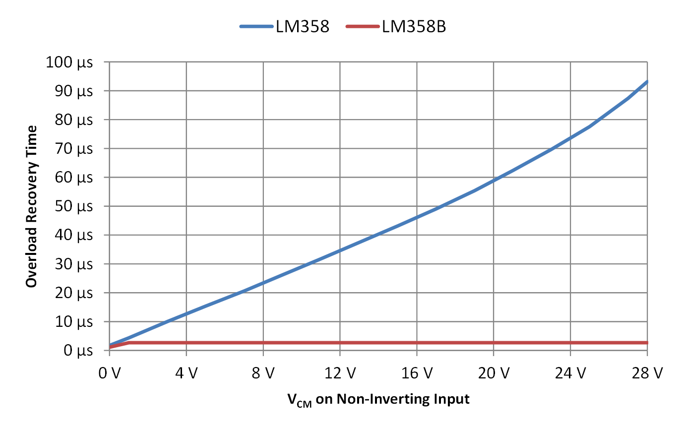
Overload recovery time is analogous to comparator propagation delay. Overload occurs when an op amp's input voltage difference is large enough such that the output reaches either the VOL or VOH level and the output no longer changes with variations in the input. Some internal node voltages will continue to change even though the op amp output is not changing. The overload condition ends when the input voltage difference is reduced to a point where the op amp returns to a linear operating region or the input voltage polarity is reversed. After the overload condition is removed, there is a finite time delay before the output can change from the VOL or VOH level. This delay is the overload recovery time. The data sheet does not specify an overload recovery time parameter. The recovery time when the output is at the VOH level is approximately 2 µs, regardless of the common mode voltage. The recovery time when the output is at VOL varies with the common mode voltage present at the non-inverting input as seen in Figure 6-1.
 Figure 6-1 Overload Recovery Time from VOL vs VIN+, VID = 200 mV, VCC = 30 V
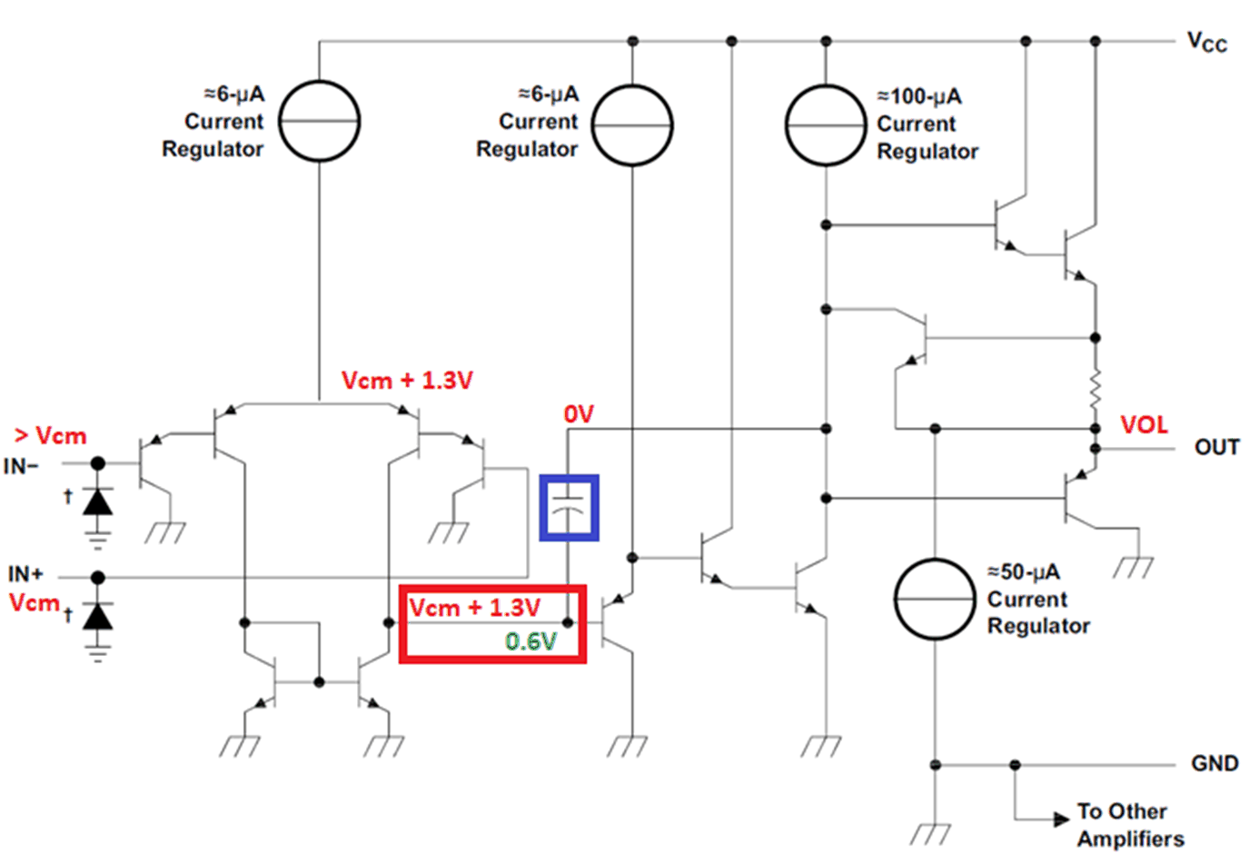
The reason for variable overload recovery time for VOL is shown in Figure 6-2. The voltage of the difference amplifier stage output (red box node) normally runs near 0.6 V when the op amp is in the linear (normal) operation mode. During a negative (VID < 0) input overload event where the output is at the VOL level, this node rises to VCM + 1.3 V while the other side of the capacitor is 0 V. This charges the capacitor to a voltage set by the voltage present on IN+ pin.
LM358B, LM2904B, LM324B, and LM2902B limit the voltage of the red box node to 1.2 V. Consequently, the overload recovery time does not increase with the IN+ voltage. When the input overload is removed, the difference amp output node voltage returns to 0.6 V. The time for this to happen depends on the input voltage difference and internal factors, such as the current of the leftmost 6-µA current regulator and the capacitance of the internal compensation capacitor highlighted in the blue box in Figure 6-2.
 Figure 6-2 Overload Recovery from VOL State
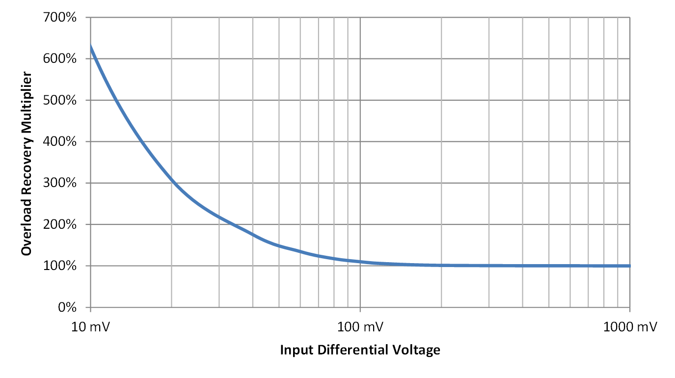
In addition to the overload recovery time of 2 µs from the VOH state or the overload recovery time in Figure 6-1 from the VOL state, the input voltage difference applied during the input recovery time is also a factor in the actual recovery time. One can multiply the internal factor time (2 µs or the time from Figure 6-1) by the scalar value in Figure 6-3 to get the final expected recovery time. VID is the voltage applied while waiting for the recovery time.
 Figure 6-3 Overload Recovery Multiplier vs Input Differential Voltage (VID)
For example, assume the LM358 output is in a VOL state, the non-inverting input is 10 V, and the inverting input is 10.05 V. If the inverting input suddenly drops to 9.98 V, then the output will start increasing after approximately 90 µs. The input common mode was 10 V, which makes the overload recovery time 30 µs, per Figure 6-1. The input difference is 10 V – 9.98 V = 20 mV which makes the multiplier 300%, per Figure 6-3. Multiply the two values; 30 µs × 300% = 90 µs. Later when the inverting input suddenly rises back to 10.05 V, the output will start decreasing after approximately 3 µs. The output was VOH, so the recovery time is 2 µs. The input difference is 10.05 V – 10 V = 50 mV, which makes the multiplier 150%, per Figure 6-3. Multiply the two values; 2 µs × 150% = 3 µs.