SLUA963B June 2020 – October 2022 UCC21710-Q1 , UCC21732-Q1 , UCC5870-Q1
- HEV/EV Traction Inverter Design Guide Using Isolated IGBT and SiC Gate Drivers
- 1Introduction
- 2HEV/EV Overview
-
3Design of HEV/EV Traction Inverter Drive Stage
- 3.1 Introduction to UCC217xx-Q1
- 3.2 Designing a Traction Inverter Drive System Using UCC217xx-Q1
- 3.3 Description of Protection Features
- 3.4 Protection Features of UCC217xx-Q1
- 3.5
UCC217xx-Q1 Protection and Monitoring Features Descriptions
- 3.5.1 Primary and Secondary Side UVLO and OVLO
- 3.5.2 Over-Current (OC) and Desaturation (DESAT) Detection
- 3.5.3 2-Level and Soft Turn-Off
- 3.5.4 Power Switch Gate Voltage (VGE/VGS) Monitoring
- 3.5.5 Power Switch Anti-Shoot-Through
- 3.5.6 Integrated Internal or External Miller Clamp
- 3.5.7 Isolated Analog-to-PWM Channel
- 3.5.8 Short-Circuit Clamping
- 3.5.9 Active Pulldown
- 3.6 Introduction to UCC5870-Q1
- 3.7 Designing a Traction Inverter Drive System Using UCC5870-Q1
- 3.8 Description of Protection Features
- 3.9 Protection Features of UCC5870-Q1
- 3.10
UCC5870-Q1 Protection and Monitoring Features Descriptions
- 3.10.1 Primary and Secondary Side UVLO and OVLO
- 3.10.2 Programmable Desaturation (DESAT) Detection and Over-Current (OC)
- 3.10.3 Adjustable 2-Level or Soft Turn-Off
- 3.10.4 Active High-Voltage Clamp
- 3.10.5 Power Switch Gate Voltage (VGE/VGS) Monitoring
- 3.10.6 Gate Threshold Voltage Monitor
- 3.10.7 Power Switch Anti-Shoot-Through
- 3.10.8 Active Short Circuit (ASC)
- 3.10.9 Integrated Internal or External Miller Clamp
- 3.10.10 Isolated Analog-to-Digital Converter
- 3.10.11 Short-Circuit Clamping
- 3.10.12 Active and Passive Pulldown
- 3.10.13 Thermal Shutdown and Temperature Warning of Driver IC
- 3.10.14 Clock Monitor and CRC
- 3.10.15 SPI and Register Data Protection
- 4Isolated Bias Supply Architecture
- 5Summary
- 6References
- 7Revision History
3.5.1 Primary and Secondary Side UVLO and OVLO
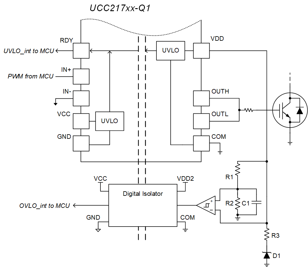
Under and over-voltage lockout (UVLO and OVLO) are used to protect the driver IC as well as monitor the voltage used to drive the power switch on the secondary side. UVLO is integrated into UCC217xx-Q1 for both the primary and secondary side supplies, VCC and VDD respectively. These are used to protect the system in case of bias supply failures. The output is pulled low if VCC or VDD drops below the UVLO threshold. Additionally, if there is a UVLO fault, the RDY pin will go HIGH. For VCC the threshold is 2.7 V with a 0.2 V band of hysteresis. The VDD UVLO threshold is 12 V, referenced to COM, with 0.8 V hysteresis. Aside from bias failures, the VDD-side UVLO is beneficial to protect the power switch. Based on the I-V characteristics of high-power IGBTs and SiC MOSFETs, if the device is driven at 12 V the conduction losses are smaller and early saturation of the device can be prevented. In this way, UVLO can be useful to prevent damaging the FET due to a drop in supply voltage.
Overvoltage lockout (OVLO) is also implemented to protect the power switch from being driven with too high of a voltage, outside of the device ratings, which could cause gate oxide breakdown or reduced lifetime. The driver IC should not be supplied with a voltage beyond the maximum ratings, as it may result in driver failure and uncertain driver output state. OLVO is implemented using external circuitry to protect the driver and power device from bias supply failure on the secondary side supply, VDD. VDD is divided down and compared to a fixed voltage reference generated by a Zener diode. When the divided voltage drops below the Zener voltage, the comparator output will switch and will be sent across the isolation barrier to the MCU.
 Figure 3-3 Integrated UVLO and External OVLO Implementation