SLUAA33A April 2020 – October 2022 BQ25970
3.1 Simplified Schematic
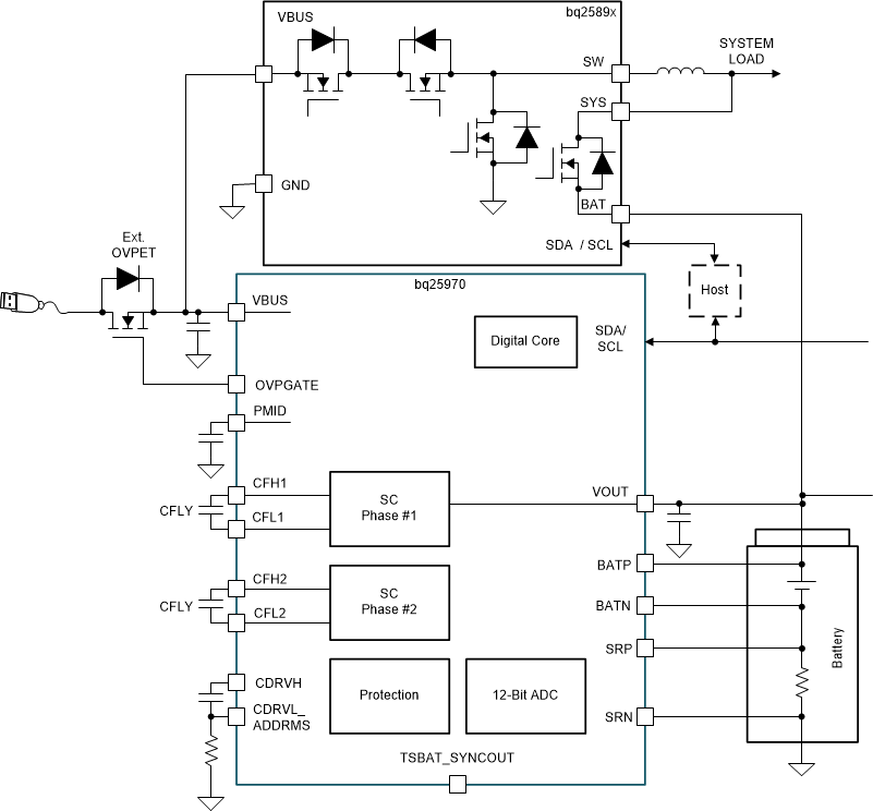
Figure 3-1 illustrates the BQ25970 simplified schematic.
 Figure 3-1 BQ25970 Simplified Schematic
- CFLY is charge pump capacitor, it is a power storage component
- The external MOSFET is used for overvoltage protection of VBUS and it can replace the dedicated OVP switch in VBUS with a low-cost MOSFET
In general, all power capacitors for BQ25970 applications should be MLCC (Multiple Layer Ceramic Capacitor) because of their smaller package, lower ESR, and lower power dissipation. The biggest shortfall of a MLCC is that the effective capacitance is derated due to DC biased voltage on the capacitor. When DC biased voltage on the MLCC increases, the effective capacitance of the MLCC will decrease accordingly. It is necessary to keep enough capacitance, in an actual design, the DC biased voltage curve vs. capacitance in the MLCC data sheet is a useful tool to find a suitable power capacitor. As Figure 3-2 shows, when DC biased voltage increases, the effective capacitance decreases quickly. Of course, the designer has to consider whether the maximum voltage that the power capacitor supports can meet an actual request. For example, if the power rail is 10 V, then the designer should choose a 16-V MLCC to avoid any failures . Meanwhile, the designer has to consider the impact of temperature on the effective capacitance because different ambient working temperatures will lead to the change of effective capacitance.
 Figure 3-2 MLCC Effective Capacitance vs DC Biased Voltage and Temperature
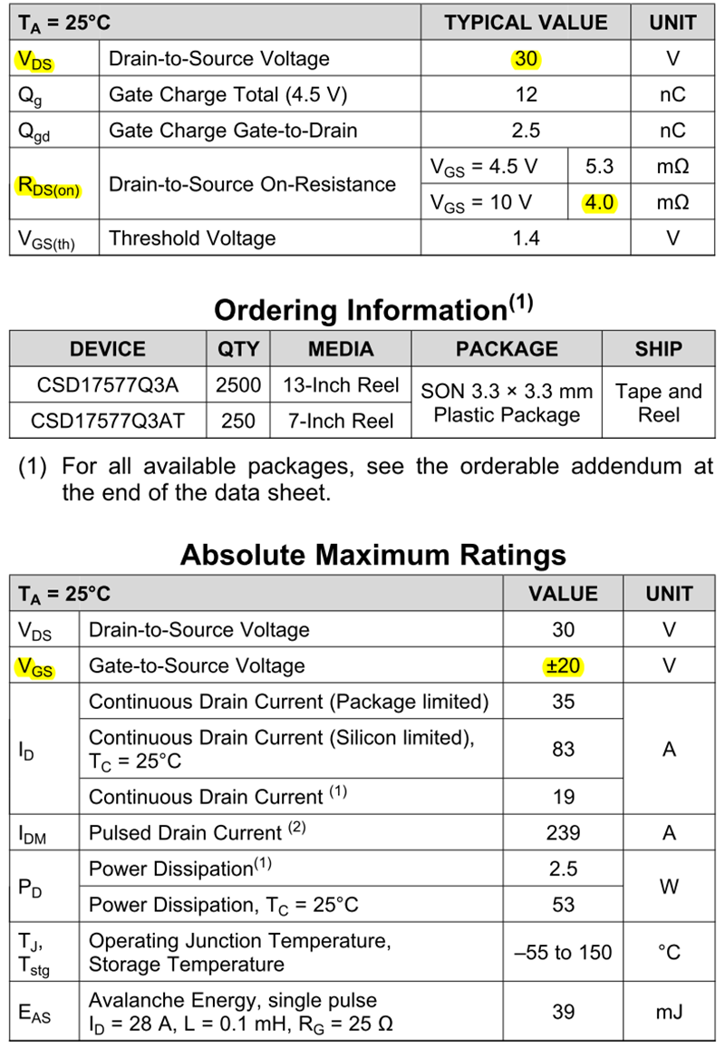
The external MOSFET will act as an OVP function, so when choosing a MOSFET, its maximum rating voltage of VDS is important. It depends on the maximum voltage on VBUS, when the voltage on VBUS exceeds the OVP setting of the BQ25970 device, this MOSFET will be turned off immediately, typically in less than 100 ns. Also, the RDS(on) of the MOSFET will impact efficiency, so a lower RDS(on) MOSFET is a good choice. Finally, the VGS of the MOSFET should be more than 10 V.
The MOSFET CSD17577Q3A specification table in (Figure 3-3) from the CSD17577Q3A 30-V N-Channel NexFET™ Power MOSFET data sheet shows: key parameters, VDS, RDS(on), and VGS.
 Figure 3-3 MOSFET Key Specification Table