SLUAA33A April 2020 – October 2022 BQ25970
1.2 BQ25970 Simplified Power Stage
The BQ25970 device adopts charge pump topology with a 2-phase interleaving fixed 50% duty-cycle, this structure can get higher efficiency because the 2-phase power stage can balance power dissipation between them.
 Figure 1-1 Ideal Charge Pump Working Process
Based on the ideal (ignore all of the impendence on power stage and power trace) working process of a charge pump as Figure 1-1 shows, the equation between VIN and VBAT can be expressed as,
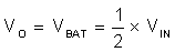
Equation 1 shows VO is always following VIN, in other words, the BQ25970 device behaves just like a kind of 2:1 voltage follower, when VIN changes, VO is changed accordingly.
 Figure 1-2 Actual Charge Pump Working Process
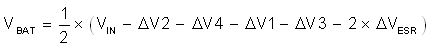
In an actual system, the impedance on the power stage and power trace cannot be ignored, as Figure 1-2 shows. The internal resistance of the BQ25970 device can be described as R1 –R4 or RDS(on) for Q1–Q4, RESR means CFLY capacitor ESR, so change Equation 1 as in Equation 2:
Some definitions can be made in the whole working cycle of the charge pump, charging and discharging as done in Equation 3, and Equation 4.


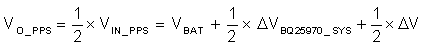
Then, substitute ΔVBQ25970_SYS into the original formula:
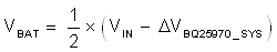
This reforms Equation 5 into Equation 6,

Since the BQ25970 device is a 2:1 charge pump, VO will be expressed as Equation 7.

To create a charger using a Programmable Power Supply (PPS) protocol, such as the Power Delivery (PD) protocol, use an output voltage set slightly higher (such as ΔV) than 2 times the calculated voltage, as in Equation 7, (VBAT + 0.5 × ΔVBQ25970_SYS). To the BQ25970 device, it does not have a feedback loop for VO, therefore, it is a kind of open loop power source, meaning that the BQ25970 device should be looked upon as a power source with non-zero internal resistance because its output voltage cannot be kept to a fixed value (for a power converter with feedback control loop, because the control loop can always keep the output as a fixed value whatever load current changes or not, meaning its internal resistance can be looked as 0, or an ideal power source). As Figure 1-3 shows, it is equivalent VO_PPS circuitry for BQ25970 output, it can be viewed as an ideal power source with internal resistance: the internal resistance is RBQ25970_SYS, the voltage of VO_PPS_Ideal equals to VO_PPS from the PPS pre-set according to PPS protocol and all of impendence on the BQ25970 and PCB trace is ignored.
 Figure 1-3 VO_PPS Equivalent Circuitry
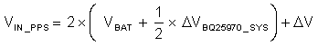
Equation 8 and Equation 9 assumes the total resistance of power trace between BQ25970 output and battery is RPower_Trace, the charging current is calculated using Equation 10:
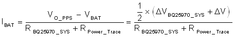
For a detailed description of RPower_Trace, see Section 3.2.
In Equation 10, either ΔV or R is changed and the charging current will be changed accordingly. If the designer can keep R or ΔV on power trace at a lower level, they will get higher efficiency at the same charging current condition.