SLUAA33A April 2020 – October 2022 BQ25970
3.2 How to Translate R on Power Trace From input to Output of BQ25970 or Reversely
As previously described, the BQ25970 device acts like a 2:1 converter, so it can be expressed with an equivalent transformer model as this section shows.


Using the same theory, Equation 13 is a re-expression of Equation 11 and Equation 12.
In Equation 13, ΔVX means the voltage drop on the power trace.

 Figure 3-4 R on Power Trace Translation
R translation from output to input:
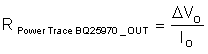
Assumes that the output power trace resistance of BQ25970 is RPower Trace_BQ25970_OUT as Figure 3-4 shows.
This can also be represented as shown in Equation 14.
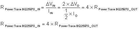
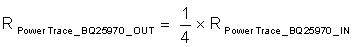
Equation 15 is an example when converted to the input resistance of the BQ25970 device.
R translation from input to output:
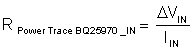
In the same way, assumes that the input power trace resistance of the BQ25970 device is RPower Trace_BQ25970_IN as Figure 3-4 shows.
This can also be represented as shown in Equation 16.
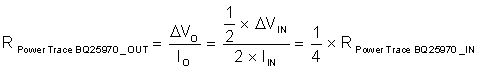
Equation 17 is an example when converted to the output resistance of the BQ25970 device,
Designers can easily evaluate the power dissipation in different power traces to improve thermal performance by using Equation 15 or Equation 18. Also, the BQ25970 device supports parallel configuration to get much higher charging current, such as 10 A or more. This method can help the designer to optimize the PCB layout of power trace and get almost the same charging current between two BQ25970 devices to get excellent thermal performance.