SLVA514C July 2014 – November 2022 TPS62125
2.3 Power Good Pin
The TPS62125 has a built-in power good (PG) function to indicate whether the output voltage has reached its appropriate level or not. The PG pin is an open-drain output that requires a pullup resistor. Because VOUT is the IC ground in this configuration, the PG pin is referenced to VOUT instead of ground, which means that the TPS62125 pulls PG to VOUT when it is low.
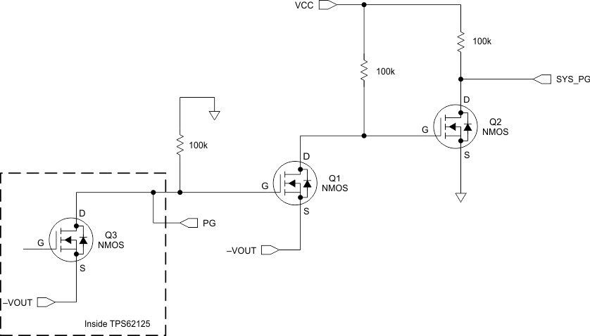
This behavior can cause difficulties in reading the state of the PG pin, because in some applications the IC detecting the polarity of the PG pin may not be able to withstand negative voltages. The level shifter circuit shown in Figure 2-4 alleviates any difficulties associated with the offset PG pin voltages by eliminating the negative output signals of the PG pin. If the PG pin functionality is not needed, it may be left floating or connected to VOUT without this circuit. Note that to avoid violating its absolute maximum rating, the PG pin should not be driven more than 6 V above the negative output voltage (IC ground).
 Figure 2-4 PG Pin Level Shifter
Inside the TPS62125, the PG pin is connected to an N-channel MOSFET (Q3). By tying the PG pin to the gate of Q1, when the PG pin is pulled low, Q1 is off and Q2 is on because its VGS sees VCC. SYS_PG is then pulled to ground.
When Q3 turns off, the gate of Q1 is pulled to ground potential turning it on. This pulls the gate of Q2 below ground, turning it off. SYS_PG is then pulled up to the VCC voltage. Note that the VCC voltage must be at an appropriate logic level for the circuitry connected to the SYS_PG net.
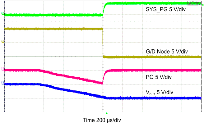
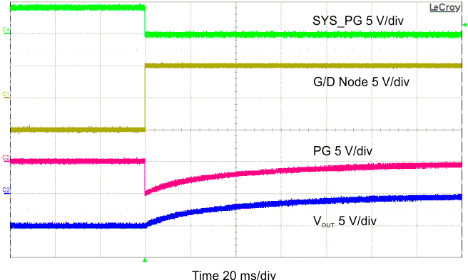
This PG pin level shifter sequence is illustrated in Figure 2-5 and Figure 2-6. The PG signal activates the PG pin level shifter circuit, and the G/D Node signal represents the shared node between Q1 and Q2. This circuit was tested with a VCC of 5 V and dual NFET Si1902DL. The SYS_PG net is the output of the circuit and goes between ground and 5 V, and is easily read by a separate device. The EN_hys pin was used to accelerate VOUT's return to 0V, when the IC is disabled.
 Figure 2-5 PG Pin Level Shifter on Startup
 Figure 2-6 PG Pin Level Shifter on Shutdown