SLVA514C July 2014 – November 2022 TPS62125
2.1 Enable Pin
The device is enabled once the voltage at the EN pin trips its threshold and the input voltage is above the UVLO threshold. The TPS62125 stops operation once the voltage on the EN pin falls below its threshold or the input voltage falls below the UVLO threshold.
Because VOUT is the IC ground in this configuration, the EN pin must be referenced to VOUT instead of ground. In the buck configuration, 1.2 V is considered a high and less than 1.15 V is considered a low. In the inverting buck-boost configuration, however, the VOUT voltage is the reference; therefore, the high threshold is 1.2 V + VOUT and the low threshold is 1.15 V + VOUT. For example, if VOUT = –5 V, then VEN is considered at a high level for voltages above –3.8 V and a low level for voltages below –3.85 V.
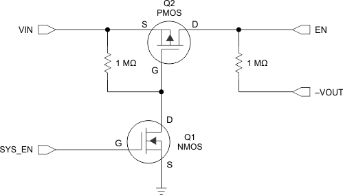
This behavior can cause difficulties enabling or disabling the part, since in some applications, the IC providing the EN signal may not be able to produce negative voltages. The level shifter circuit shown in Figure 2-1 alleviates any difficulties associated with the offset EN threshold voltages by eliminating the need for negative EN signals. If disabling the TPS62125 is not desired, the EN pin may be directly connected to VIN without this circuit.

The positive signal that originally drove EN is instead tied to the gate of Q1 (SYS_EN). When Q1 is off (SYS_EN grounded), Q2 sees 0 V across its VGS and also remains off. In this state, the EN pin sees –5 V which is below the low-level threshold and disables the device.
When SYS_EN provides enough positive voltage to turn Q1 on (VGS threshold as specified in the MOSFET datasheet), the gate of Q2 sees ground through Q1. This drives the VGS of Q2 negative and turns Q2 on. Now, VIN ties to EN through Q2 and the pin is above the high-level threshold, turning the device on. Be careful to ensure that the VGD and VGS of Q2 remain within the MOSFET ratings during both the enabled and disabled states. Failing to adhere to this constraint can result in damaged MOSFETs.
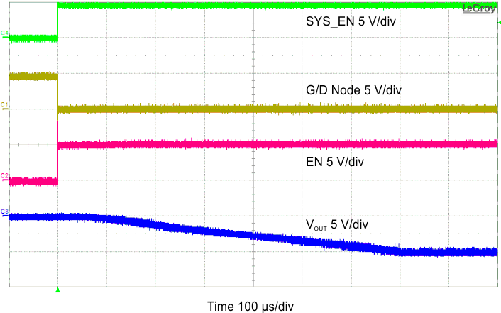
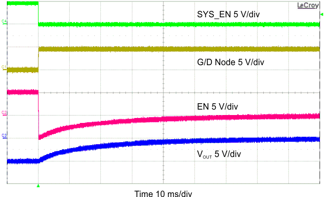
The enable and disable sequence is illustrated in Figure 2-2 and Figure 2-3. The SYS_EN signal activates the enable circuit, and the G/D Node signal represents the shared node between Q1 and Q2. This circuit was tested with a 5-V SYS_EN signal and dual N/PFET Si1029X. The EN signal is the output of the circuit and goes from VIN to VOUT properly enabling and disabling the device. The PG pin was used as an output discharge to accelerate VOUT's return to 0V, when the IC is disabled.
 Figure 2-2 Enable Sequence
 Figure 2-3 Disable Sequence