SLVA514C July 2014 – November 2022 TPS62125
2.4 Discharging the Output Voltage
If the TPS62125 is disabled in a light-load or no-load condition, the PG or EN_hys pins can accelerate VOUT's return to 0 V by providing an additional discharge path. When the IC is disabled via the EN pin, the PG and EN_hys pins are connected to the device ground (VOUT) through an internal MOSFET. Placing a resistor between ground and the PG or EN_hys pins creates a discharge path to ground. If the EN_hys pin is already being used to adjust the enable thresholds, do not use this pin as a discharge path. If the PG pin is already being used, do not use this pin as a discharge path.
The added resistor should be sized to limit the current into the PG or EN_hys pin to a safe level. The PG output typically has an internal resistance of 600 Ω and a 400-Ω minimum. The maximum sink current into the PG pin is 10 mA. In order to limit the discharge current to the maximum allowable sink current into the PG pin, an external resistor is calculated using:
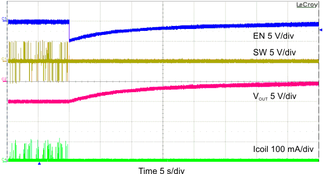
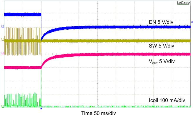
Use a 100-Ω resistor for a –5-V output. Figure 2-7 and Figure 2-8 illustrate the purpose of the PG/EN_hys pin discharge path – the output voltage returns to 0 V quicker with the discharge circuit.
 Figure 2-7 Shutdown at No Load and No PG Pin Discharge
 Figure 2-8 Shutdown at No Load and PG Pin Discharge of 100 Ohm