SLVUB62B June 2017 – November 2020
- Trademarks
- 1 About this Manual
- 2 Information About Cautions and Warnings
- 3 Items Required for Operation
- 4 Introduction
-
5 Setup
- 5.1
Switch, Push Button, Connector, and Test Point Descriptions
- 5.1.1 Power Path Jumper Configuration
- 5.1.2 DP Source Receptacle
- 5.1.3 S1 HRESET Push-Button
- 5.1.4 S6 SPI MISO Pull Down Button
- 5.1.5 S3: FTDI Enable and Disable
- 5.1.6 S2: SPI , I2C, and BusPowerZ Configurations
- 5.1.7 J1: Barrel Jack Power Connector
- 5.1.8 Barrel Jack Detect
- 5.1.9 USB Type B Connector (J11)
- 5.1.10 USB Type-CConnector (J2)
- 5.1.11 USB Micro B Connector (J9)
- 5.1.12 TP13 (5 V), TP8 (3.3 V), and TP12 (1.2 V)
- 5.1.13 Aardvark Connector (J10)
- 5.1.14 TP10, TP11, TP15, TP16, TP17, TP18, TP9: GND Test Points
- 5.1.15 TP1, TP2, TP3 and TP4 – CC1 and CC2 Test Points
- 5.1.16 TP14 (PA and PB): VBUS Test Point
- 5.1.17 TP7, TP6, and TP5: A-VAR, B-VAR, and System Power Test Points Respectively
- 5.1.18 J3 and J4 (Bottom of EVM): Signal Headers
- 5.2 LED Indicators Description
- 5.1
Switch, Push Button, Connector, and Test Point Descriptions
- 6 Using the TPS65988EVM
- 7 Connecting the EVM
- 8 REACH Compliance
- 9 TPS65988EVM Schematic
- 10TPS65988EVM Board Layout
- 11TPS65988EVM Bill of Materials
- 12Revision History
10 TPS65988EVM Board Layout
Figure 9-1 through Figure 10-12 contain the PCB layouts of the TPS65988EVM.
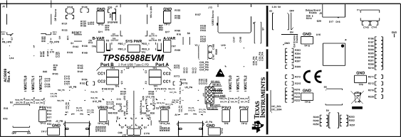 Figure 10-1 TPS65988EVM Top Overlay
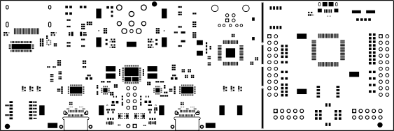 Figure 10-2 TPS65988EVM Solder
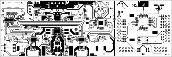 Figure 10-3 TPS65988EVM Top Layer SSTXRX1
 Figure 10-4 TPS65988EVM GND Plane 1
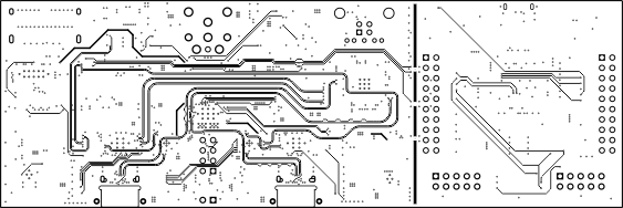 Figure 10-5 TPS65988EVM High Speed
 Figure 10-6 TPS65988EVM GND Plane 2
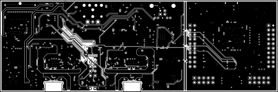 Figure 10-7 TPS65988EVM Power 1
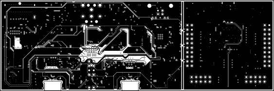 Figure 10-8 TPS65988EVM Power 2
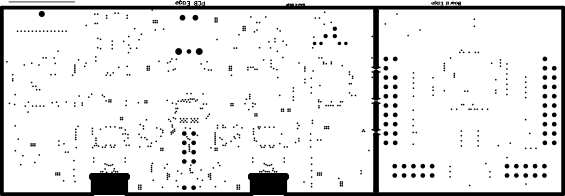 Figure 10-9 TPS65988EVM GND Plane 3
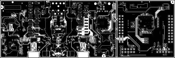 Figure 10-10 TPS65988EVM SSTXRX2
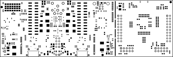 Figure 10-11 TPS65988EVM Solder Mask
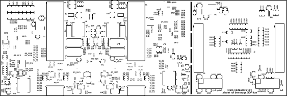 Figure 10-12 TPS65988EVM Bottom Layer Component View