SLVUB62B June 2017 – November 2020
- Trademarks
- 1 About this Manual
- 2 Information About Cautions and Warnings
- 3 Items Required for Operation
- 4 Introduction
-
5 Setup
- 5.1
Switch, Push Button, Connector, and Test Point Descriptions
- 5.1.1 Power Path Jumper Configuration
- 5.1.2 DP Source Receptacle
- 5.1.3 S1 HRESET Push-Button
- 5.1.4 S6 SPI MISO Pull Down Button
- 5.1.5 S3: FTDI Enable and Disable
- 5.1.6 S2: SPI , I2C, and BusPowerZ Configurations
- 5.1.7 J1: Barrel Jack Power Connector
- 5.1.8 Barrel Jack Detect
- 5.1.9 USB Type B Connector (J11)
- 5.1.10 USB Type-CConnector (J2)
- 5.1.11 USB Micro B Connector (J9)
- 5.1.12 TP13 (5 V), TP8 (3.3 V), and TP12 (1.2 V)
- 5.1.13 Aardvark Connector (J10)
- 5.1.14 TP10, TP11, TP15, TP16, TP17, TP18, TP9: GND Test Points
- 5.1.15 TP1, TP2, TP3 and TP4 – CC1 and CC2 Test Points
- 5.1.16 TP14 (PA and PB): VBUS Test Point
- 5.1.17 TP7, TP6, and TP5: A-VAR, B-VAR, and System Power Test Points Respectively
- 5.1.18 J3 and J4 (Bottom of EVM): Signal Headers
- 5.2 LED Indicators Description
- 5.1
Switch, Push Button, Connector, and Test Point Descriptions
- 6 Using the TPS65988EVM
- 7 Connecting the EVM
- 8 REACH Compliance
- 9 TPS65988EVM Schematic
- 10TPS65988EVM Board Layout
- 11TPS65988EVM Bill of Materials
- 12Revision History
5.1.1.2 TPS65987D Jumper Configuration
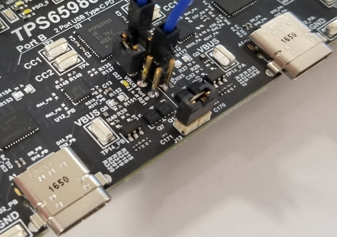
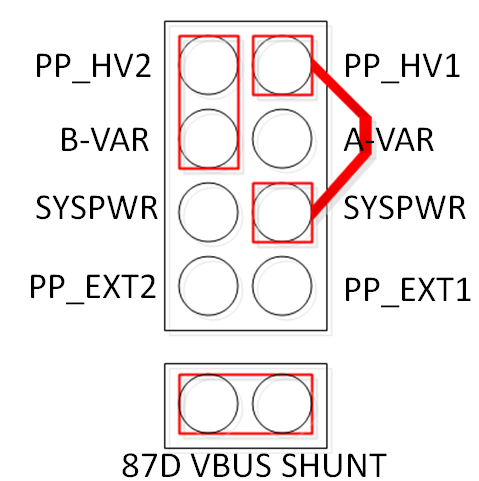
To use the TPS65988EVM to perform as a TPS65987D, the jumpers on J11 and J12 needs to be adjusted. Place a jumper on J12 to short the two VBUS nodes together. In this use case, one of the internal power paths is used as a source path and the other internal power path is used as a sink path. The TPS65987D supports one Type-C port and contains 2 internal power paths. The TPS65988 can be configured to act as a TPS65987D through the use of a TPS65987D Configuration Template in the TPS6598x Application Customization Tool. In this configuration, PPHV2 is used as the Source path for the Type-C port, it is connected to the net B-Var which is the Variable DC/DC used for Port B in the TPS65988 configuration. PPHV1 is used for the Sink path on the TPS65987D. PPHV1 connects to the net SYSPWR in this configuration. Refer to Figure 5-3 and Figure 5-4 for the TPS65987D Jumper Configuration. When the TPS65988EVM is configured as a TPS65987D, only Port A is functional.
 Figure 5-3 TPS65987D Jumper Configuration
 Figure 5-4 TPS65987D Jumper Configuration Net Names