SLVUB62B June 2017 – November 2020
- Trademarks
- 1 About this Manual
- 2 Information About Cautions and Warnings
- 3 Items Required for Operation
- 4 Introduction
-
5 Setup
- 5.1
Switch, Push Button, Connector, and Test Point Descriptions
- 5.1.1 Power Path Jumper Configuration
- 5.1.2 DP Source Receptacle
- 5.1.3 S1 HRESET Push-Button
- 5.1.4 S6 SPI MISO Pull Down Button
- 5.1.5 S3: FTDI Enable and Disable
- 5.1.6 S2: SPI , I2C, and BusPowerZ Configurations
- 5.1.7 J1: Barrel Jack Power Connector
- 5.1.8 Barrel Jack Detect
- 5.1.9 USB Type B Connector (J11)
- 5.1.10 USB Type-CConnector (J2)
- 5.1.11 USB Micro B Connector (J9)
- 5.1.12 TP13 (5 V), TP8 (3.3 V), and TP12 (1.2 V)
- 5.1.13 Aardvark Connector (J10)
- 5.1.14 TP10, TP11, TP15, TP16, TP17, TP18, TP9: GND Test Points
- 5.1.15 TP1, TP2, TP3 and TP4 – CC1 and CC2 Test Points
- 5.1.16 TP14 (PA and PB): VBUS Test Point
- 5.1.17 TP7, TP6, and TP5: A-VAR, B-VAR, and System Power Test Points Respectively
- 5.1.18 J3 and J4 (Bottom of EVM): Signal Headers
- 5.2 LED Indicators Description
- 5.1
Switch, Push Button, Connector, and Test Point Descriptions
- 6 Using the TPS65988EVM
- 7 Connecting the EVM
- 8 REACH Compliance
- 9 TPS65988EVM Schematic
- 10TPS65988EVM Board Layout
- 11TPS65988EVM Bill of Materials
- 12Revision History
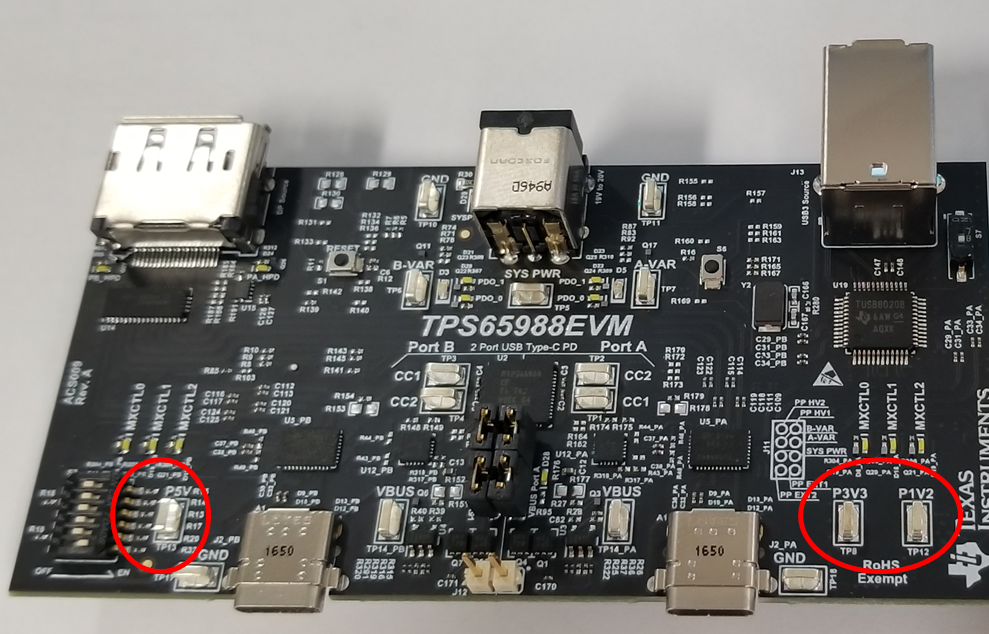
5.1.12 TP13 (5 V), TP8 (3.3 V), and TP12 (1.2 V)
Use the TP13, TP8, and TP12 test points to measure the output voltage of the onboard DC/DC converters. These DC/DC converters produce the required voltage rails for full functionality of the EVM including power delivery, powering internal and external circuits, and so forth. These test points allow the user to verify the system supplies on the TPS65988EVM. LDO_1V8 is internally generated for internal circuitry. Use P3V3 to supply VIN_3V3 which then supplies LDO_3V3. Also, use LDO_3V3 as a low-power output for external flash memory. In bus-powered conditions, or self-powered conditions, P3V3 and LDO_3V3 are active. P3V3 has the ability to operate at 4 V to compensate for IR drop through the USB Type-C cable. The P5V supply can operate at 4.5 V at 100% duty cycle, but it is intended to supply the 5 V at 3 A when the barrel jack or system power is connected to the EVM. P5V powers PP_CABLE for both ports as well as the VBUS current sense IC for both ports. Figure 5-27 highlights these test points.
 Figure 5-27 TP13 (5 V), TP8 (3.3 V), and TP12 (1.2 V)