SLVUBB4B November 2017 – February 2023
- Abstract
- Trademarks
- 1 Topologies Window
- 2 FET Losses Calculator
- 3 Load Step Calculator
- 4 Capacitor Current Sharing Calculator
- 5 AC/DC Bulk Capacitor Calculator
- 6 RCD-Snubber Calculator for Flyback Converters
- 7 RC-Snubber Calculator
- 8 Output Voltage Resistor Divider
- 9 Dynamic Analog Output Voltage Scaling
- 10Dynamic Digital Output Voltage Scaling
- 11Unit Converter
-
12Loop Calculator
- 12.1 Inputs
- 12.2
Transfer Functions
- 12.2.1 Output Impedance Transfer Function
- 12.2.2 Transfer Function VMC Buck Power Stage
- 12.2.3 Transfer Function CMC Buck Power Stage
- 12.2.4 Transfer Function CMC Boost Power Stage
- 12.2.5 Transfer Function CMC Inverting Buck-Boost Power Stage
- 12.2.6 Transfer Function CMC Forward Power Stage
- 12.2.7 Transfer Function CMC Flyback Power Stage
- 12.2.8 Transfer Function Closed Loop
- 12.2.9 Transfer Function Isolated Type II Compensation Network With a Zener Clamp
- 12.2.10 Transfer Function Isolated Type II Compensation Network Without a Zener Clamp
- 13Filter Designer
- 14Additional Information
- 15Revision History
2 FET Losses Calculator
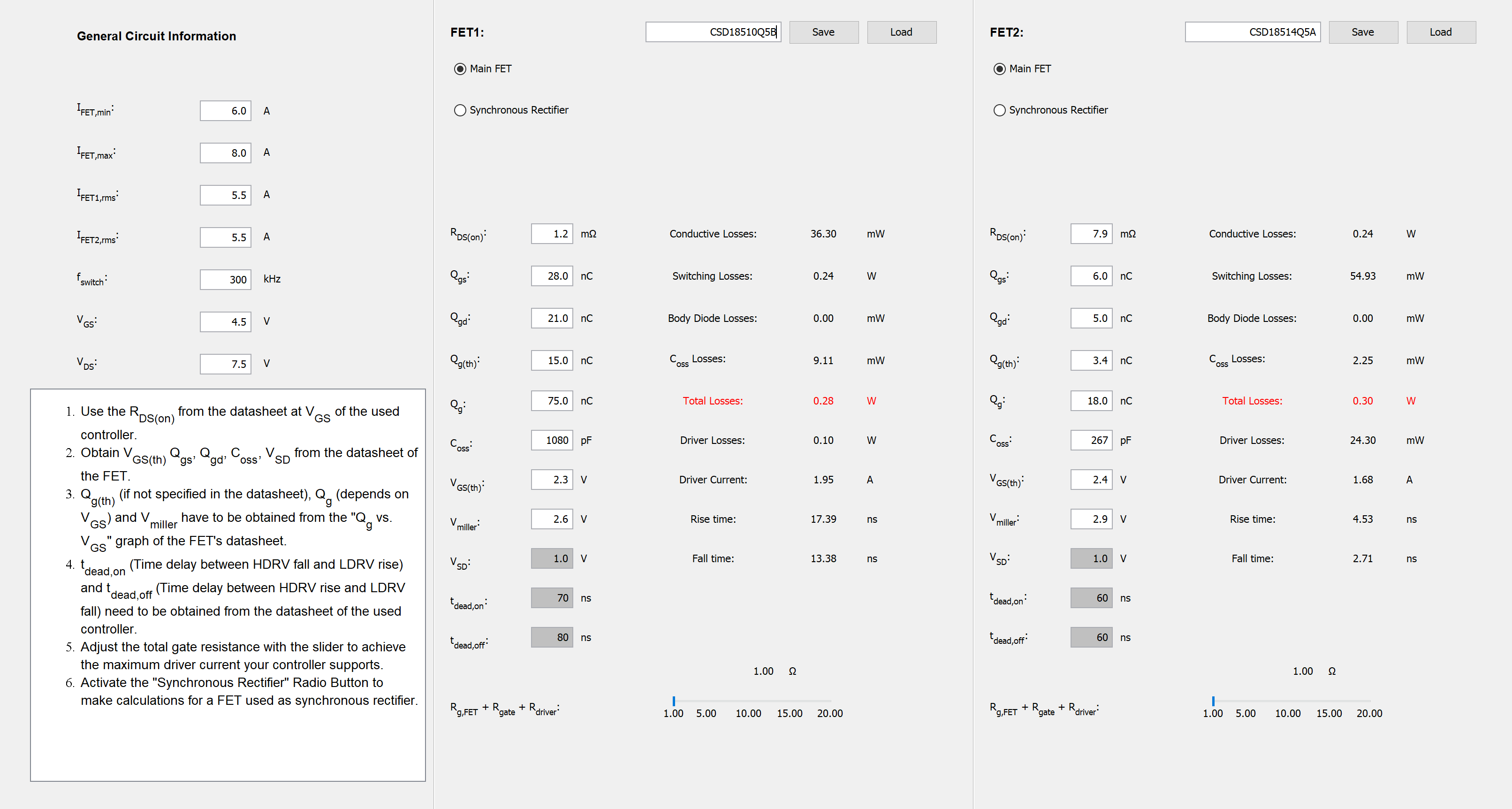
The FET Losses Calculator lets the user either compare two different FETs or calculate losses for the main FET and a synchronous rectifier in a hard-switching power stage. #SLVUBB44807 shows the FET Losses Calculator window.
The Quasi-resonant Flyback, LLC-Half-Bridge, LLC-Full-Bridge, and Phase-Shifted Full-Bridge are resonant topologies. Manual inputs can provide more accurate results.
 Figure 2-1 FET
Losses Calculator Window
Figure 2-1 FET
Losses Calculator WindowTo attain the most accurate results, it is important to determine the gate drive voltage (VGS) of the power management controller since the values for Qg (which is relevant for driver losses) and RDS(on) are dependent on this voltage and must be obtained from graphs in the data sheet of the FET.
The different losses which can be seen in the FET of a power supply are conducted losses, switching losses, Coss losses, and body diode losses. Reverse recovery losses are neglected, but can become significant at high switching frequencies.
Conductive losses:
Switching losses:
Coss losses:
Body Diode losses:
The total losses for the main FET can be calculated as indicated in #SLVUBB44493
For synchronous rectifiers, the switching losses equal zero due to soft switching, but during the dead time the body diode is conducting. So the total losses result as indicated in #SLVUBB48072:
Additionally, driver losses occur in the power management controller, which can be calculated as shown in #SLVUBB44947:
Power management controllers typically have a limited amount of gate drive current they can source and sink. Therefore, it is important to adjust the total resistance in the gate drive path so the resulting gate drive current is equal to or smaller than the limit in the data sheet.