SLVUBB4B November 2017 – February 2023
- Abstract
- Trademarks
- 1 Topologies Window
- 2 FET Losses Calculator
- 3 Load Step Calculator
- 4 Capacitor Current Sharing Calculator
- 5 AC/DC Bulk Capacitor Calculator
- 6 RCD-Snubber Calculator for Flyback Converters
- 7 RC-Snubber Calculator
- 8 Output Voltage Resistor Divider
- 9 Dynamic Analog Output Voltage Scaling
- 10Dynamic Digital Output Voltage Scaling
- 11Unit Converter
-
12Loop Calculator
- 12.1 Inputs
- 12.2
Transfer Functions
- 12.2.1 Output Impedance Transfer Function
- 12.2.2 Transfer Function VMC Buck Power Stage
- 12.2.3 Transfer Function CMC Buck Power Stage
- 12.2.4 Transfer Function CMC Boost Power Stage
- 12.2.5 Transfer Function CMC Inverting Buck-Boost Power Stage
- 12.2.6 Transfer Function CMC Forward Power Stage
- 12.2.7 Transfer Function CMC Flyback Power Stage
- 12.2.8 Transfer Function Closed Loop
- 12.2.9 Transfer Function Isolated Type II Compensation Network With a Zener Clamp
- 12.2.10 Transfer Function Isolated Type II Compensation Network Without a Zener Clamp
- 13Filter Designer
- 14Additional Information
- 15Revision History
12 Loop Calculator
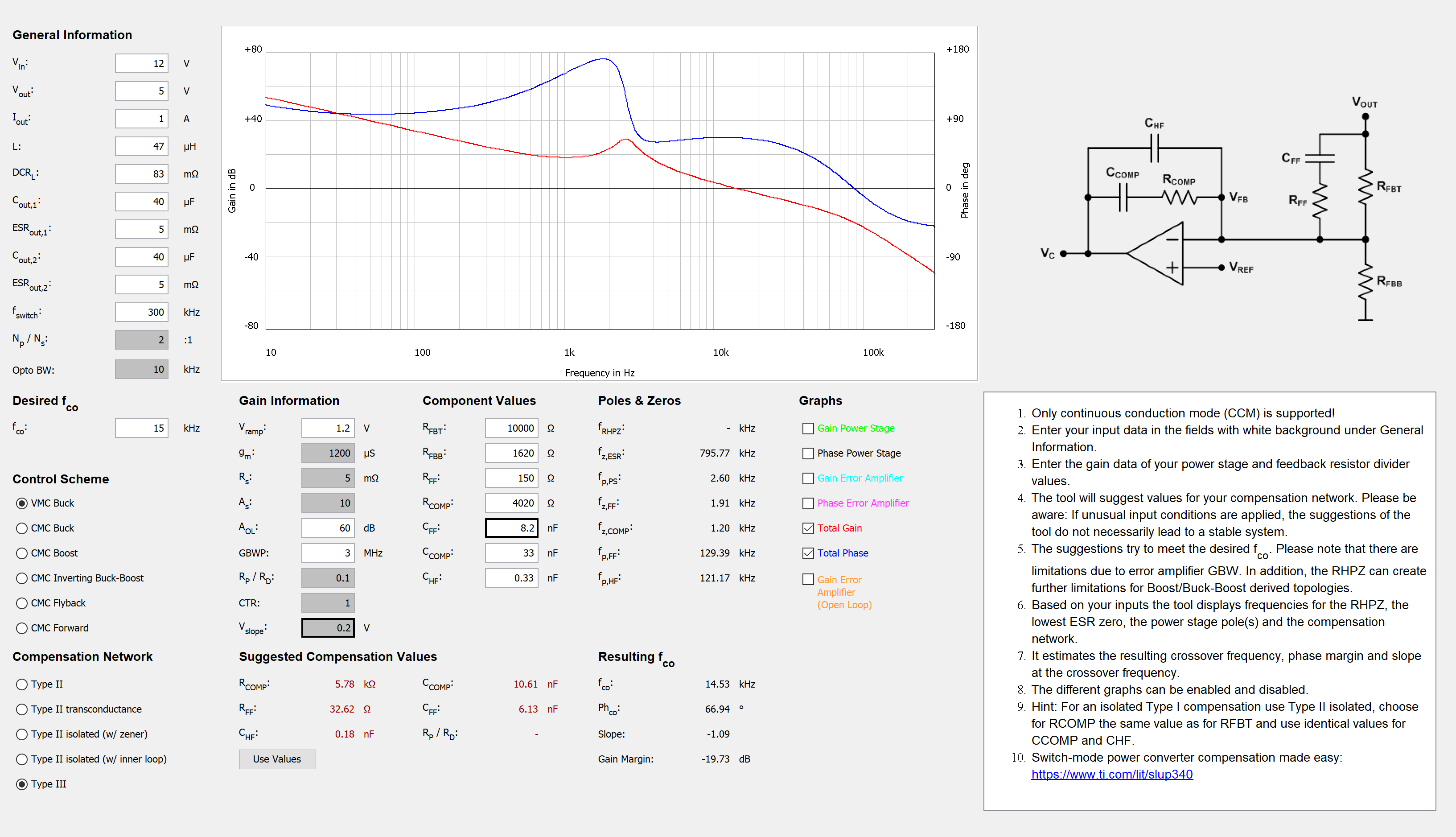
The Loop Calculator can help power supply designers with the compensation network for voltage mode controlled (VMC) buck converters or current mode controlled (CMC) buck, boost, inverting buck-boost, forward, and flyback converters operating in continuous conduction mode (CCM). The transfer functions have been simplified, thus the results give a first-order approximation of how the Bode plot of the power supply will appear. #T5147377-38 shows the Loop Calculator window.
 Figure 12-1 Loop Calculator Window
The following steps apply when using the Loop Calculator.
- Select the topology/control scheme and the type of compensation for the design with the radio buttons in the bottom-left corner. Typically, only the VMC buck needs a Type III Compensation. For all CMC topologies, a Type II Compensation is usually sufficient.
- Fill in all input fields with white background. If the Loop Calculator is started from one of the supported topologies, applicable values from the topologies window will directly transfer to the Loop Calculator window.
- Under General Information (from the schematic) sum the capacitance of the same output capacitor types and calculate their effective ESR. The DC-biasing effect for ceramic capacitors must be considered because it can have a major impact on the accuracy of the gain and phase plot of the power stage.
- Enter the Gain Information (from the schematic and the data sheet for the controller).
- Fill in the values for RFBT and RFBB. With this information the Loop Calculator can suggest values for the compensation network of the entered power supply design.
The compensation network suggestions are calculated as follows:
If unusual input conditions are applied, the suggestions of the tool do not necessarily lead to a stable system.
- Compensation zeroes are placed on the pole of the transfer function of the power stage (L and Cout double pole for VMC, Rout and Cout single pole for CMC).
- Compensation poles are placed on the lower of either half of the switching frequency or the ESR zero for Buck derived topologies.
- Compensation poles are placed on the lower of either the right half plane zero (RHPZ) frequency or the ESR zero frequency for Boost/Buck-Boost derived topologies.
- The maximum achievable crossover frequency is approximately two decades below the GBWP (gain bandwidth product) of the error amplifier. The gain of the compensation network should never go above the open loop gain of the error amplifier. Otherwise, the error amplifier will be clipping.
- For Boost/Buck-Boost derived topologies the desired crossover frequency is automatically set to 1/5 of the RHPZ frequency.