SNAA386 November   2023 CDCE6214 , CDCE6214-Q1 , CDCE6214Q1TM , LMK00301 , LMK00304 , LMK00306 , LMK00308 , LMK00334 , LMK00334-Q1 , LMK00338 , LMK03318 , LMK03328 , LMK3H0102 , LMK6C , LMK6H , LMKDB1108 , LMKDB1120


  1.   1
  2.   Abstract
  3.   Trademarks
  4. 1Introduction
  5. 2Introduction to PCIe
    1. 2.1 The PCIe Link
  6. 3PCIe Clocking Architectures
    1. 3.1 Common Clock Architecture
    2. 3.2 Separate Reference Architecture
    3. 3.3 Spread Spectrum Clocking
    4. 3.4 PCIe REFCLK Topology
    5. 3.5 Noise Folding
  7. 4PCIe Clocking Specifications
    1. 4.1 REFCLK Output Format
    2. 4.2 PCIe Jitter Requirements
    3. 4.3 PCIe Time Domain Requirements
  8. 5REFCLK Measurement Technique
    1. 5.1 Clock Generator Measurement Results
      1. 5.1.1 PNA Measurement Result without SSC
      2. 5.1.2 PCIe Filtered PNA Result without SSC
      3. 5.1.3 PNA Measurement Result, With SSC
      4. 5.1.4 PCIe Filtered PNA Result, With SSC
      5. 5.1.5 Time Domain PCIe Measurement Result
    2. 5.2 Clock Buffer Measurement Results
      1. 5.2.1 PNA Measurement Result
      2. 5.2.2 PCIe Filtered PNA Result
      3. 5.2.3 Time Domain PCIe Measurement Result
  9. 6Texas Instruments Products with PCIe Compliance
  10. 7Summary
  11. 8References

PNA Measurement Result, With SSC

Figure 5-3 is the phase noise plot of the LMK3H0102 output clock as measured by the PNA when SSC is enabled. The SSC is configured for –0.5% down-spread modulation. The 12 kHz to 20 MHz phase jitter is higher as SSC adds jitter, but much of this is filtered out when applying the PCIe filters. For CCS and SRIS, spurs from the fundamental frequency and harmonics are removed only up to 2 MHz. This is done to minimize removal of non-SSC related spurs.
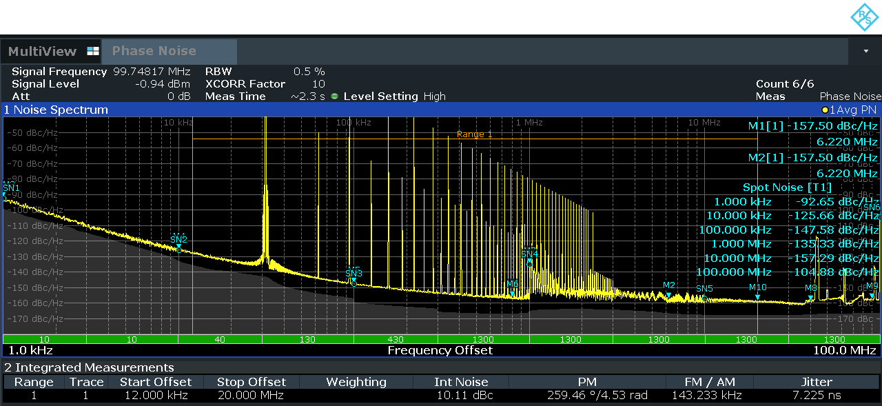
GUID-20231107-SS0I-CCN1-8JH5-NJSTHPMWFCBN-low.png Figure 5-3 LMK3H0102 Phase Noise with SSC