SNAA386 November 2023 CDCE6214 , CDCE6214-Q1 , CDCE6214Q1TM , LMK00301 , LMK00304 , LMK00306 , LMK00308 , LMK00334 , LMK00334-Q1 , LMK00338 , LMK03318 , LMK03328 , LMK3H0102 , LMK6C , LMK6H , LMKDB1108 , LMKDB1120
5.2.3 Time Domain PCIe Measurement Result
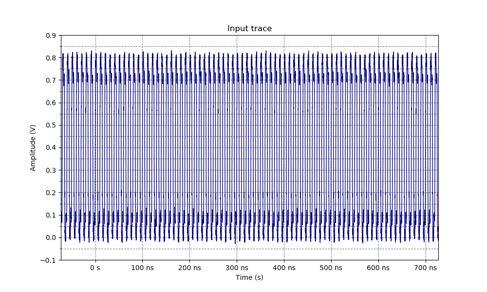
Figure 5-6 is the time domain capture of the OUT0_P and OUT0_N outputs of the LMKDB1120 as measured by the oscilloscope. These results are exported to text files, which can be read by the Texas Instruments PCIe Reference Clock Analysis Tool and analyzed for compliance.
 Figure 5-6 LMKDB1102 PCIe Time Domain
Capture
Figure 5-6 LMKDB1102 PCIe Time Domain
CaptureTable 5-6 shows the result of the oscilloscope measurement after analysis. For the LMKDB1120, all of the parameters meet the limits specified in Table 4-2.
Table 5-6 LMKDB1120 PCIe Time Domain
Results
| Parameter | Units | Minimum | Average | Maximum | Limit | Status |
|---|---|---|---|---|---|---|
| VCross | mV | 334.15 | 346.91 | 361.14 | 250 mV to 550 mV | Pass |
| VHigh | mV | 746.784 | 746.784 | 150 mV | Pass | |
| VLow | mV | –54.042 | –54.042 | –150 mV | Pass | |
| VRingback | mV | 557.354 | 586.954 | 100 mV | Pass | |
| Period | ns | 9.981 | 9.996 | 10.022 | 9.847 ns to 10.203 ns | Pass |
| Duty Cycle | % | 49.343 | 49.493 | 49.663 | 40% to 60% | Pass |
| VOvershoot | mV | 69.48 | 84.82 | 300 mV | Pass | |
| VUndershoot | mV | –67.09 | –82.29 | –300 mV | Pass | |
| Rising Edge Rate | V/ns | 2.067 | 2.336 | 2.615 | 0.6 V/ns to 4.0 V/ns | Pass |
| Falling Edge Rate | V/ns | 1.974 | 2.2 | 2.629 | 0.6 V/ns to 4.0 V/ns | Pass |