SNIA053 june 2023 TMP61-Q1
2.6 Schematic
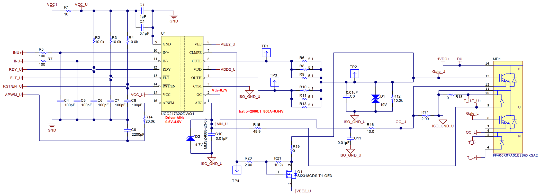
The Figure 2-11 shows the portion of the TIDA-020030 reference design schematic used in this application note. The highlighted portion of the schematic is shown in Figure 2-12 is the primary focus of the test in this application note.

Figure 2-11 Full Schematic
 Figure 2-12 Isolated Gate Driver Circuit
Note that J3 in Figure 2-11 is used to apply the inputs to the isolated gate driver as described in the following.
The UCC21732-Q1 isolated gate driver circuit (U1) drives the high side of the IGBT module (MD1). The output pins OUTH (pin 4) and OUTL (pin6) drive the drain of the MOSFET through Gate_U (Pin 13). The isolated gate driver outputs are verified through test points TP1 and TP3. An analog PWM signal from a host MCU is driven to IN+ (pin 10) of the isolated gate driver. This PWM signal is set to an 80% duty cycle at 15 kHz. IN– (pin 11) of the isolated gate driver is connected to GND. An external voltage is applied to HVDC+ (pin 14) of the IGBT module, with pin N grounded, and the switching monitored on pin U.