SNOA930C March 2015 – May 2021 LDC0851 , LDC1001 , LDC1001-Q1 , LDC1041 , LDC1051 , LDC1101 , LDC1312 , LDC1312-Q1 , LDC1314 , LDC1314-Q1 , LDC1612 , LDC1612-Q1 , LDC1614 , LDC1614-Q1 , LDC2112 , LDC2114 , LDC3114 , LDC3114-Q1
2.2 Number of Turns
 Figure 2-4 Flat Circular Spiral Inductor
For a single-layer PCB spiral inductor, Mohan’s Equation, as discussed in Reference [1], is useful for understanding how inductance is related to coil geometry. This equation can be used to calculate the overall inductance of a coil for various geometries:
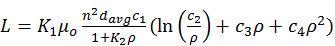
where
- K1 and K2 are geometry dependent, based on the shape of the inductor
- μo is the permeability of free space, 4π×10−7
- n is the number of turns of the inductor
- davg is the average diameter of the turns = (dOUT + dIN)/2
- ρ = (dOUT – dIN)/(dOUT + dIN), and represents the fill ratio of the inductor – small values of ρ are a hollow inductor (dOUT ≈ dIN), while large values correspond to (dOUT ≫ dIN)
- ci are layout dependent factors based on the geometry (for a circle, use c1 = 1.0, c2 = 2.46, c3 = 0, c4 = 0.20), refer to [1] for additional shapes
As the total inductance is proportional to the number of turns, adjusting the number of turns is an effective control on the total inductance. However, when adding inner turns (which reduces the inner diameter), the davg value begins to decrease, which reduces the additional inductance from the extra turns. For most applications, the ratio of dIN/dOUT must be greater than 0.3 for a higher inductor Q. The reason for this guideline is that the inner turns, which do not have a significant area, do not contribute significantly to the overall inductance while they still increase RS. However, for applications where the target is very close to the sensor, such as touch-on-metal, a ratio as low as 0.05 is often acceptable, as the inner turns provide increased sensitivity. Refer to Reference [2] for more information.
 Figure 2-5 Inductance Versus Number of Turns for 18-mm Circular Inductor
A key limitation on the number of turns that can be added is the practical minimum PCB trace width – a common value is 0.1 mm (or 0.004 in.). Under this constraint, with each increase of 2 mm in sensor diameter up to 5 additional turns can be added to a PCB inductor.
In Figure 2-5, it can be seen that the first few turns contribute the most inductance, while the last few turns contribute less inductance. This example with an 18-mm outer diameter coil with 0.15-mm trace width and trace spacing shows that the total inductance levels off at approximately 20 turns.