SNVA037F April 2001 – February 2022 LM3477 , LM3488
5 Layout Fundamentals
Good layout for DC-DC converters can be implemented by following a few simple design guidelines:
- Place the power components (catch diode, inductor, and filter capacitors) close together. Make the traces between them short.
- Use wide traces between the power components and for power connections to the DC-DC converter circuit.
- Connect the ground pins of the input and output filter capacitors and catch diode as close as possible using generous component-side copper fill as a pseudo-ground plane. Then, connect this to the ground-plane with several vias.
- Arrange the power components so that the switching current loops curl in the same direction.
- Route high-frequency power and ground return as direct continuous parallel paths.
- Separate noise sensitive traces, such as the voltage feedback path, from noisy traces associated with the power components.
- Ensure a good low-impedance ground for the converter IC.
- Place the supporting components for the converter IC, such as compensation, frequency selection and charge-pump components, as close to the converter IC as possible but away from noisy traces and the power components. Make their connections to the converter IC and its pseudo-ground plane as short as possible.
- Place noise sensitive circuitry, such as radio-modem IF blocks, away from the DC-DC converter, CMOS digital blocks, and other noisy circuitry.
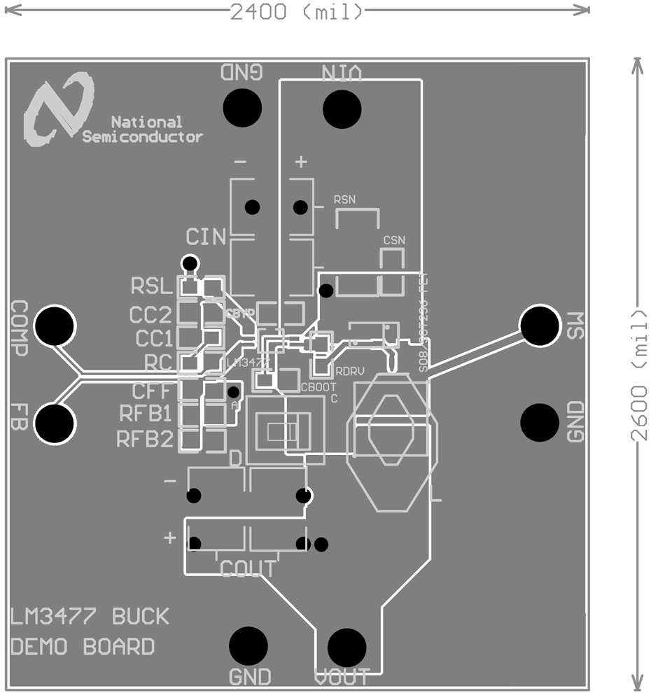
 Figure 5-1 LM3477 Evaluation Board PCB Layout (Top Side)
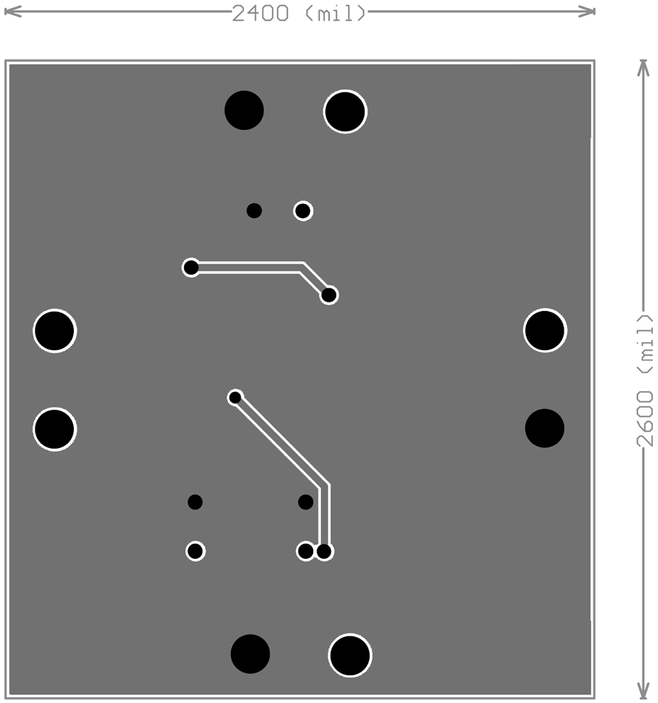
 Figure 5-2 LM3477 Evaluation Board PCB Layout (Bottom Side)