SNVA037F April 2001 – February 2022 LM3477 , LM3488
2 Performance
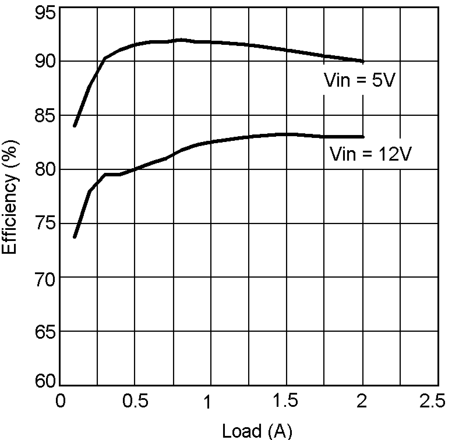
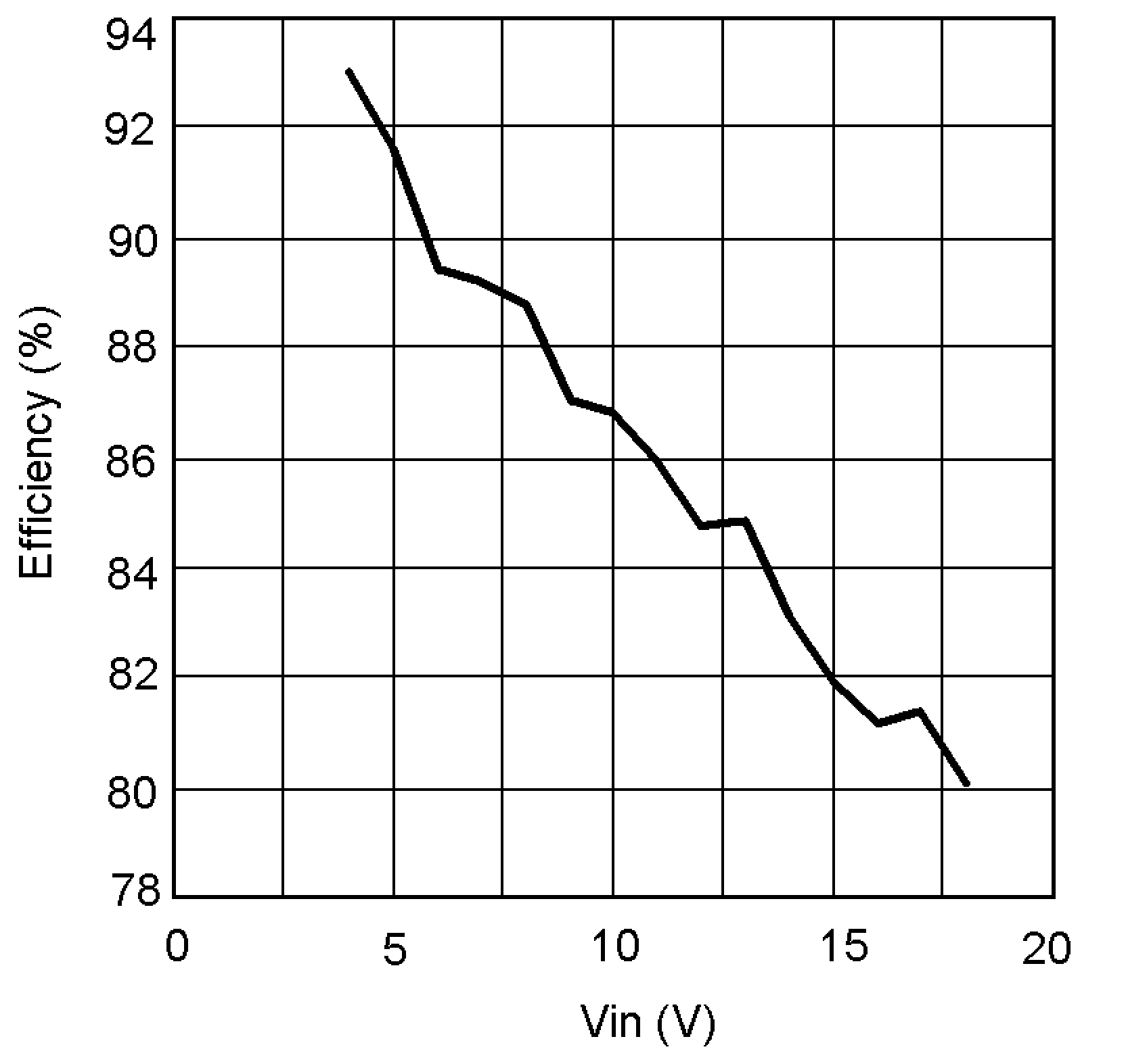
Figure 2-1 to Figure 2-2 show some benchmark data taken from the circuit above on the LM3477 evaluation board. This evaluation board can also be used to evaluate a buck regulator circuit optimized for a different operating point or to evaluate a trade-off between cost and some performance parameter. For example, the conversion efficiency can be increased by using a lower RDS(ON) MOSFET, ripple voltage can be lowered with lower ESR output capacitors, and the hysteretic threshold can be changed as a function of the RSN and RSL resistors.
The conversion efficiency can be increased by using a lower RDS(ON) MOSFET, however, it drops as input voltage increases. The efficiency reduces because of increased diode conduction time and increased switching losses. Switching losses are due to the Vds × Id transition losses and to the gate charge losses, both of which can be lowered by using a FET with low gate capacitance. At low duty cycles, where most of the power loss in the FET is from the switching losses, trading off higher RDS(ON) for lower gate capacitance will increase efficiency.
 Figure 2-1 Efficiency vs Load VOUT =
3.3 V
 Figure 2-2 Efficiency vs VIN
VOUT = 3.3 V, IOUT = 2 A
Figure 2-2 Efficiency vs VIN
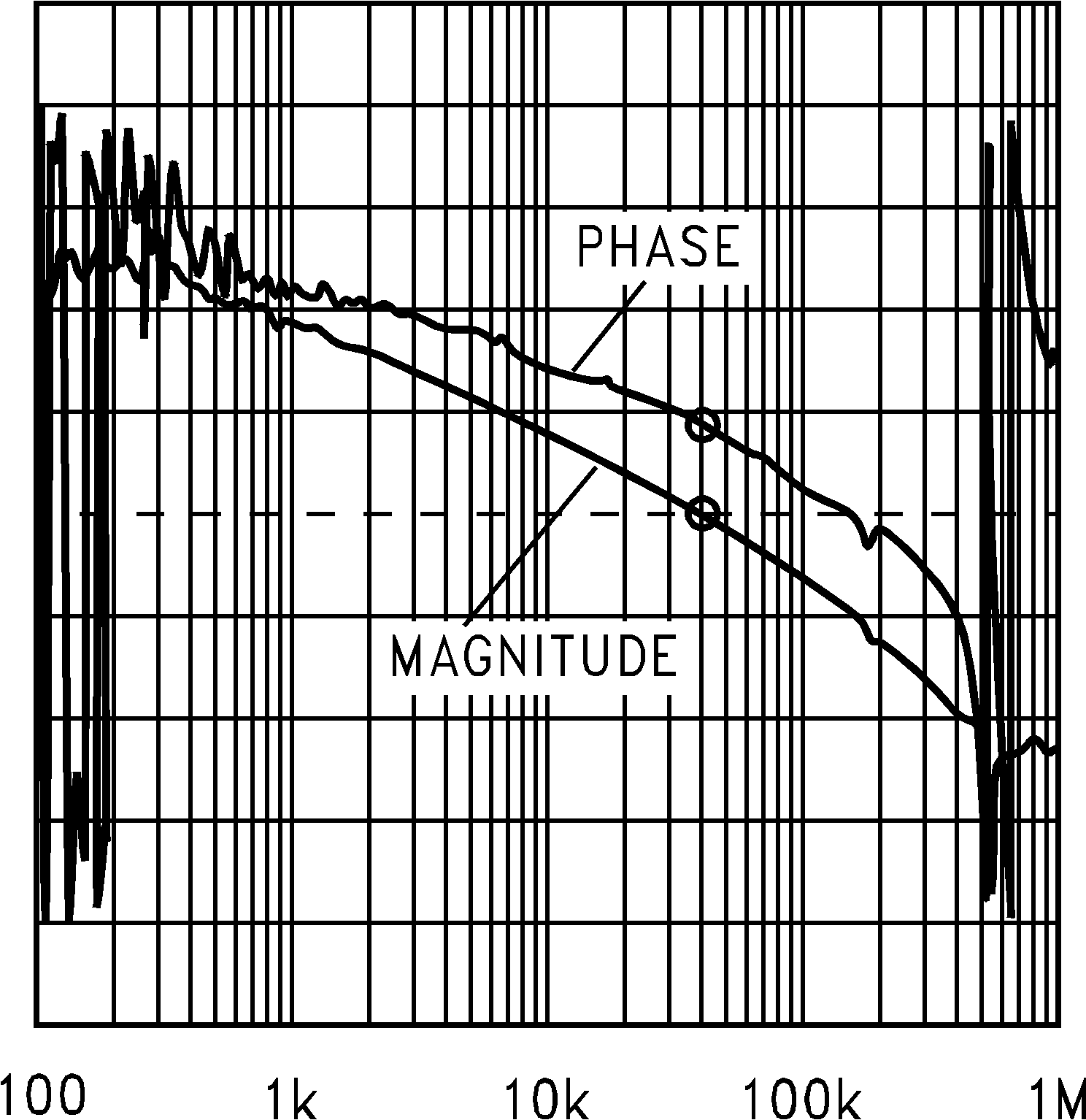
VOUT = 3.3 V, IOUT = 2 AFigure 3-1 shows a bode plot of LM3477 open loop frequency response using the external components listed in Table 1-1.
