SNVA856B May 2020 – October 2022 LM63615-Q1 , LM63625-Q1 , LM63635-Q1 , LMR33620 , LMR33620-Q1 , LMR33630 , LMR33630-Q1 , LMR33640 , LMR36006 , LMR36015 , TPS54360B , TPS54560B
- Working With Inverting Buck-Boost Converters
- Trademarks
- 1 Introduction
- 2 Inverting Buck-Boost Converter
- 3 Basic Operation
- 4 Operating Considerations of a Buck Based Inverting Buck-Boost
- 5 Component Selection for the IBB
- 6 General Considerations
- 7 Auxiliary Functions
- 8 Design Examples
- 9 Summary
- 10References
- 11Revision History
7.3 Power-Good Flag Level Shift
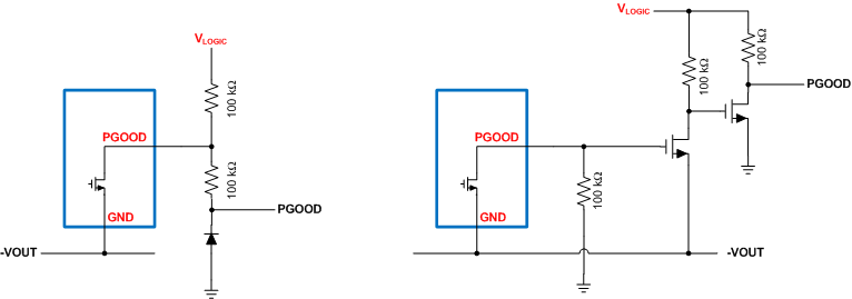
Many applications require a "power-good" or "reset" flag from the DC/DC converter to alert the µC that the output voltage is within specification. The circuits shown in Figure 7-3 can be used to level shift the status flag to the system ground.
 Figure 7-3 Power-Good Flag Level Shifters
The circuit on the left is simple, however the PGOOD signal swings below ground by a diode drop. The circuit on the right is slightly more complicated, giving a PGOOD signal that swings to zero volts. In either case the PGOOD signal swings high to the user defined VLOGIC level. Be sure to check the Absolute Maximum Rating on the power good pin from the buck data sheet. For the circuit on the left, the power good pin must withstand VLOGIC + |VOUT|. For the other design the power good must withstand |VOUT|.