SNVA856B May 2020 – October 2022 LM63615-Q1 , LM63625-Q1 , LM63635-Q1 , LMR33620 , LMR33620-Q1 , LMR33630 , LMR33630-Q1 , LMR33640 , LMR36006 , LMR36015 , TPS54360B , TPS54560B
- Working With Inverting Buck-Boost Converters
- Trademarks
- 1 Introduction
- 2 Inverting Buck-Boost Converter
- 3 Basic Operation
- 4 Operating Considerations of a Buck Based Inverting Buck-Boost
- 5 Component Selection for the IBB
- 6 General Considerations
- 7 Auxiliary Functions
- 8 Design Examples
- 9 Summary
- 10References
- 11Revision History
7.2 Synchronizing Input Level Shift
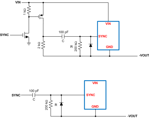
Some regulators have a synchronizing input for locking the switching frequency to the system clock. One of the level shifters shown in Figure 7-2 can be used to provide this function.
 Figure 7-2 Synchronization Level Shifters
The lower schematic shows a simple solution, but requires a low impedance drive signal. The solution in the upper schematic although more complex allows the use of ordinary logic drive. Also, this solution requires that the SYNC input can withstand VIN + |VOUT|. In all cases the RC time constant should be much longer than the switching period.