SNVA856B May 2020 – October 2022 LM63615-Q1 , LM63625-Q1 , LM63635-Q1 , LMR33620 , LMR33620-Q1 , LMR33630 , LMR33630-Q1 , LMR33640 , LMR36006 , LMR36015 , TPS54360B , TPS54560B
- Working With Inverting Buck-Boost Converters
- Trademarks
- 1 Introduction
- 2 Inverting Buck-Boost Converter
- 3 Basic Operation
- 4 Operating Considerations of a Buck Based Inverting Buck-Boost
- 5 Component Selection for the IBB
- 6 General Considerations
- 7 Auxiliary Functions
- 8 Design Examples
- 9 Summary
- 10References
- 11Revision History
8.2 Converting +5 V to –5 V at 1 A
The design objectives are shown in Table 8-2 .
| VIN | VOUT | IOUT | SWITCHING FREQUENCY |
|---|---|---|---|
| +5 V | -5 V | 1 A | 400 kHz |
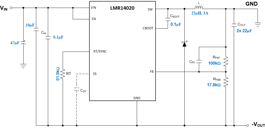
The maximum voltage seen by the regulator is 10 V. The inductor is calculated based on 30% of 1 A, or 0.3 A. We find an inductance of 22 µH; a standard value. With an efficiency of 0.85, the peak and valley currents are 2.33 A and 2.02 A, respectively. The average inductor current is about 2.18 A. The LMR14020 has a minimum peak current limit of 2.5 A. We will use the LMR14020 for the this example. So our inductor will be 22 µH rated for at least 3 A.
For CIO we use the data sheets recommendation of one 10-µF capacitor and one 0.1-µF capacitor rated for at least 16 V. For CIN a small aluminum electrolytic of 47µF to 100µF can be used. For a +5 V, 2 A design the data sheet recommends one 47 µF or two 22 µF ceramic capacitors. This is a good starting point for our IBB. Allow space on the PCB for extra output capacitors is they are required to improve the load transient response and/or the loop stability. The value of CBOOT is 0.1 µF.
The LMR14020 requires a feed-back voltage divider. From the data sheet we arrive at: RFBT = 100 kΩ and RFBB = 17.8 kΩ. Also, leave a place on the PCB for a CFF capacitor so that the loop stability can be optimized. To set the switching frequency to 400 kHz, we use an RT = 61.9 kΩ. The SS input can be used to increase the soft-start time if desired; otherwise leave it open. If using a soft-start capacitor on this pin, it should be returned directly to the device GND pin. If enable control is not needed, connect the EN input to VIN. Otherwise one of the level shifters shown previously can be used to control the EN input.
Once the design is completed, measure the efficiency to ensure that the converter can supply the required load current over the entire range of input voltage and ambient temperature. The complete schematic for the +5 V to –5 V design using the LMR14020 is shown in Figure 8-2.
 Figure 8-2 +5 V to –5 V, 1-A Design with the LMR14020