SPRAC76G November 2022 – February 2024 AM5706 , AM5708 , AM5716 , AM5718 , AM5726 , AM5728 , AM5729 , AM5746 , AM5748 , AM5749 , AM620-Q1 , AM623 , AM625 , AM625-Q1 , AM625SIP , AM6411 , AM6412 , AM6421 , AM6422 , AM6441 , AM6442 , AM6526 , AM6528 , AM6546 , AM6548
- 1
- Sitara Processor Power Distribution Networks: Implementation and Analysis
- Trademarks
- 1Introduction
- 2Guidelines for PCB Stack-Up
- 3Physical Layout Optimization of the PDN
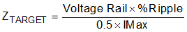
- 4Static PDN Analysis (IR Drop Optimization)
- 5Dynamic Analysis of PCB PDN
- 6Checklist for PDN
- 7Implementation Examples and PDN Targets
- Revision History
5 Dynamic Analysis of PCB PDN
The typical elements of the PDN are shown in Figure 5-1; which includes the chip-level power distribution with thin-oxide decoupling capacitors. The package-level power distribution with planes and mid-frequency decoupling capacitors; and the board-level (for example, PCB) power distribution with planes, low-frequency ceramic and bulk decoupling capacitors, and the voltage regulator module (VRM).
") Figure 5-1 Components of a Typical Power Distribution Network (PDN)
Figure 5-1 Components of a Typical Power Distribution Network (PDN)The frequency ranges covered by these elements are shown in Figure 5-2. As the primary focus is on optimizing the PCB PDN for high performance, the methodology is developed around the areas over which the PCB designer has control over and can influence early in the design phase.
 Figure 5-2 Decoupling Frequency Range of PCB Components
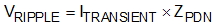
The VRM/PMIC/SMPS (or simply voltage regulator device) is the first major component of the PDN. It observes its output voltage and adjusts the amount of current being supplied to keep the voltage constant. Most common voltage regulators make this adjustment on the order of milliseconds to microseconds. They are effective at maintaining output voltage for events at all frequencies from DC to a few kilohertz (depending on the regulator dynamic response time). For all transient events that occur at frequencies above this range, there is a time delay before the voltage regulator can respond to the new level of demand. During this time delay the rail suffers from voltage droop. A power delivery network has an impedance (ZPDN) associated with the path from the voltage regulator module to the processor. The magnitude of noise (voltage ripple) seen on a given power rail is proportional to the impedance (ZPDN) and the transient current (ITRANSIENT) draw associated with that rail.
Based on Ohm’s Law,
Typically the transient current is application-specific and is determined by a particular switching scenario. As a board designer, you have the ability to minimize the voltage ripple by reducing ZPDN either by reducing the inductance, or by maximizing the capacitance. To ensure that the voltage ripple noise is within the processor’s specification, the ZPDN must be designed to meet a certain impedance, referred to as the target impedance (ZTARGET). Using frequency domain target impedance method (FDTIM) to describe the behavior of a power delivery system has been widely accepted.
The key concept of the FDTIM is the determination of the target impedance ZTARGET (see Equation 3) for the power rail under consideration. For reliable operation of a power delivery system, its impedance spectrum needs to be maintained below the target value at the frequencies from DC to FMAX (see Figure 5-2). FMAX is the point in frequency after which adding a reasonable number of decoupling capacitors does not bring the power rail impedance |ZEFF| below the target impedance (ZTARGET) due to the dominance of the parasitic planar spreading inductance and package inductances.