SSZT632 September 2018 LM53625-Q1 , LM53635-Q1 , LMR33630 , LMR33630-Q1 , LMR36006 , LMR36006-Q1 , LMR36015 , LMR36015-Q1
It is well known that printed circuit board (PCB) layout is pivotal to help reduce electromagnetic interference (EMI) from DC/DC buck or boost converters. This is critical for automotive applications that require ultra-low EMI, such as automotive gateway modules and radar sensing systems.
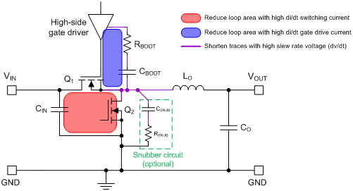
The schematic of Figure 1 illustrates two critical loops for a synchronous buck converter circuit. Minimizing the power loop area in the layout is essential because of its proportionality to parasitic inductance and related H-field propagation.
 Figure 1 Simplified Synchronous Buck
Converter Schematic with Critical Loops and Traces Identified for EMI
Figure 1 Simplified Synchronous Buck
Converter Schematic with Critical Loops and Traces Identified for EMIAlso important is the boot capacitor loop shown in Figure 1. An optional series boot resistor, designated RBOOT, controls the turn-on speed of the high-side MOSFET. The boot resistor slows the gate drive current profile and thus reduces the SW voltage and current slew rates during MOSFET turn-on. Another option is an RC snubber from SW to GND. Of course, snubbers and gate resistors increase power dissipation, leading to a trade-off between EMI and efficiency. Other techniques are required to mitigate EMI, given that efficiency and thermal performance are also important.
DC/DC Converter Package and Pinout Design
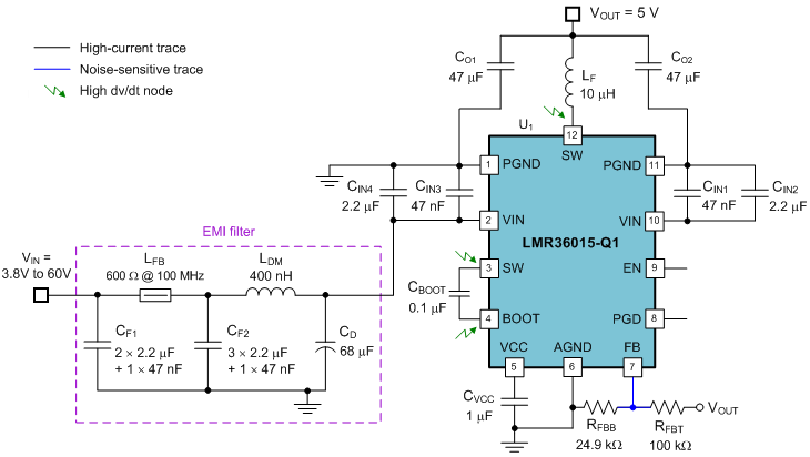
 Figure 2 DC/DC Converter with
EMI-optimized Package and Pinout. Included Is a Two-stage EMI Input
Filter
Figure 2 DC/DC Converter with
EMI-optimized Package and Pinout. Included Is a Two-stage EMI Input
Filter1. Pinout
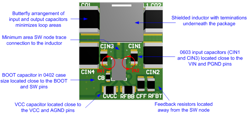
 Figure 3 Power Stage Layout Routed Only
on the Top Layer of the PCB
Figure 3 Power Stage Layout Routed Only
on the Top Layer of the PCBThe output current loops are similarly optimized as well by using two ceramic output caps, CO1 and CO2, one on each side of the inductor. Having two parallel ground return paths from the output splits the return current in two, helping to mitigate output noise and ground bounce effect.
The SW pin in located at the center of the IC such that the radiated e-field is shielded by adjacent VIN and PGND pins on both sides of the IC. GND plane copper shields the polygon pour connecting the IC’s SW pin to the inductor terminal. The single-layer SW and BOOT layout implies that vias with high dv/dt do not appear on the bottom side of the PCB. This avoids e-field coupling to the reference ground plane during the EMI test.
2. Package
 Figure 4 Wire-bond QFN (a) and HotRod
FCOL (b) Package Construction Comparison
Figure 4 Wire-bond QFN (a) and HotRod
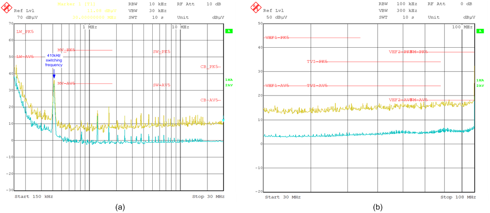
FCOL (b) Package Construction ComparisonFigure 5 shows the conducted emissions measured from 150kHz to 108MHz for the circuit in Figure 3. The results are in compliance with EN 55025 Class 5 requirements for automotive, even without a CM choke, snubbers or metal case shielding.
 Figure 5 Conducted Emissions Results
Meeting EN 550525 Class 5 Limits: 150kHz to 30MHz – Includes LW, MW, SW and CB
Bands (a); 30MHz to 108MHz – Includes VHF, TV and FM Bands (b)
Figure 5 Conducted Emissions Results
Meeting EN 550525 Class 5 Limits: 150kHz to 30MHz – Includes LW, MW, SW and CB
Bands (a); 30MHz to 108MHz – Includes VHF, TV and FM Bands (b)Summary
Additional Resources
-
Read the TI E2ETM Behind the Wheel blog, “There are more ways than you think to reduce conducted EMI.”
-
Take the EMI training webinar, “Reduce EMI and shrink solution size with HotRod packaging.”
-
Examine these reference designs from the TI Designs library:
-
Download these white papers:
-
Order the evaluation modules for the LMR36015-Q1, LMR33630-Q1 and LM53635-Q1 family of HotRod converters.