SSZT933 october 2017 DAC38RF80 , TPS82130

Do you have a need for a negative voltage rail to bias a radio frequency (RF) sampling data converter such as the DAC38RF80? Most applications don’t require the generation of a negative voltage, but you do need it to bias the current sinks in many types of high performance digital-to-analog converters (DACs). In a multi-channel, multi-device system the total negative supply current requirements can add up; a critical need is to have the right device which can supply these currents in multi-channel systems such as base-stations.
Key system considerations are to meet the total current requirements, low noise, small size and high efficiency; these are requirements for negative-voltage power supplies for data converters which often further challenge system designers to find a power supply that meets their needs in these areas without compromise.
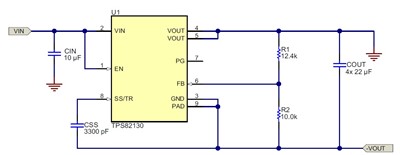
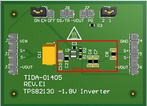
TI Designs are tested and proven reference designs that address such design challenges for specific systems. The 3V to 15.2V Input, 2A, -1.8V Inverting Power Module Reference Design for up to 125°C demonstrates a 2A inverting buck-boost converter. As a bonus, this design uses a simple and highly integrated power module, occupying only 50mm2 of printed circuit board (PCB) area. Figure 1 shows the schematic, while Figure 2 shows the PCB layout.
 Figure 1 2A Inverting Buck-boost
Schematic
 Figure 2 2A Inverting Buck-boost
PCB Layout
Figure 2 2A Inverting Buck-boost
PCB LayoutThe 2A of output current provided is enough to power as many as four data converters with a single power supply. This provides critical space savings in base stations and test and measurement equipment, where numerous data converters are used in a single system to increase data throughput.
In addition to saving precious PCB space, a power module greatly reduces the required design effort, simplifies external component selection by reducing the number of components, and enables a much simpler and faster PCB layout. The TPS82130 power module used in the reference design switches at 2MHz. This reduces the size of the power inductor, allowing its integration into the power module. This integration means there is one fewer component in the bill of materials (BOM) to select, order and stock as well, as one fewer component occupying PCB space.
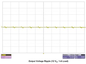
A high switching frequency also reduces the output voltage ripple down to nearly unmeasurable levels, as shown in Figure 3. Providing such a low-noise negative voltage allows the data converter to operate at its full performance without distortion. In typical base station applications, you will not need a post-DC/DC linear regulator (LDO) to reduce the noise further.
 Figure 3 Output Voltage Ripple of the
Inverting Power Module Reference Design
Figure 3 Output Voltage Ripple of the
Inverting Power Module Reference DesignSimple, tested, high power, low noise. What else do you need in your negative-voltage power solutions?