SWRU612 December 2023 CC3300 , CC3301 , CC3351
- 1
- Abstract
- Trademarks
- 1Introduction
-
2Schematic Considerations
- 2.1 Schematic Reference Design
- 2.2 Power Supply
- 2.3 Clock Source
- 2.4 Radio Frequency (RF)
- 2.5 Digital Interfaces
- 3Layout Considerations
3.5 Power Supplies
The power supplies, ground traces, and the decoupling capacitors are important for having an optimal layout. Since the decoupling capacitors can be close to the RF pins and traces of the device and power supplies, traces must be thick enough to support the necessary current to the device.
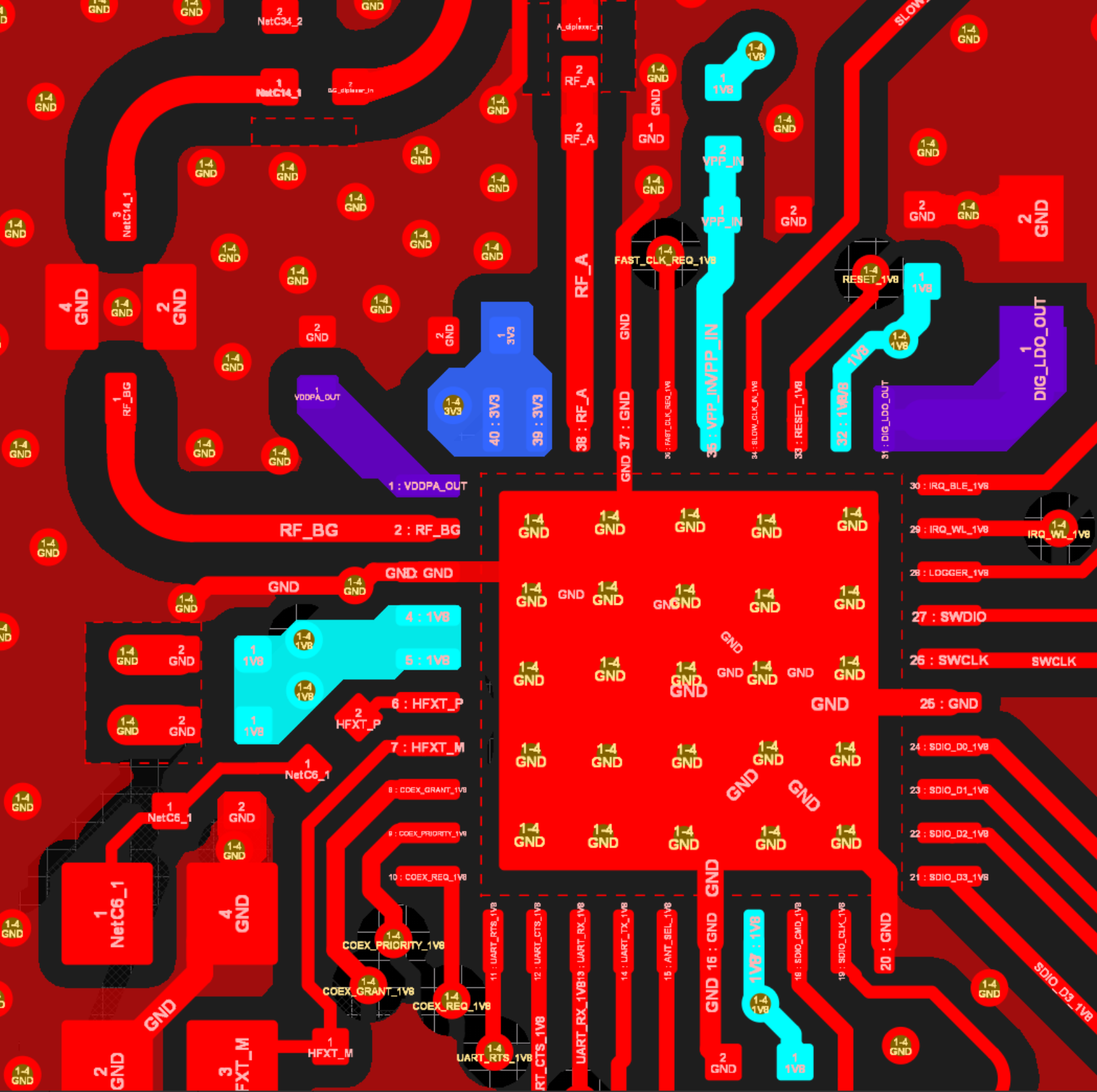
- PA_LDO_OUT (pin 1): It is suggested to have the decoupling capacitor close to the device pin, as well as a thick enough trace to have a low impedance path to the capacitor. For a visual representation, see Figure 3-13.
- VDDA_IN1 and VDDA_IN2 (pins 4 and 5): The supply side of the decoupling capacitors must be shorted together with a polygon region with two power vias (one for each decoupling capacitor). The ground side of each capacitor must go directly to ground by separate vias (not shorted together), and be isolated from the rest of the ground plane on the top layer.
- For the 1.8V power delivery, a thick trace or power plane must be used to carry the required amount of current consumption in VDD_MAIN_IN, VIO, VDDA_IN1, VDDA_IN2, and VPP_IN combined. For max current consumption, see Table 2-2.
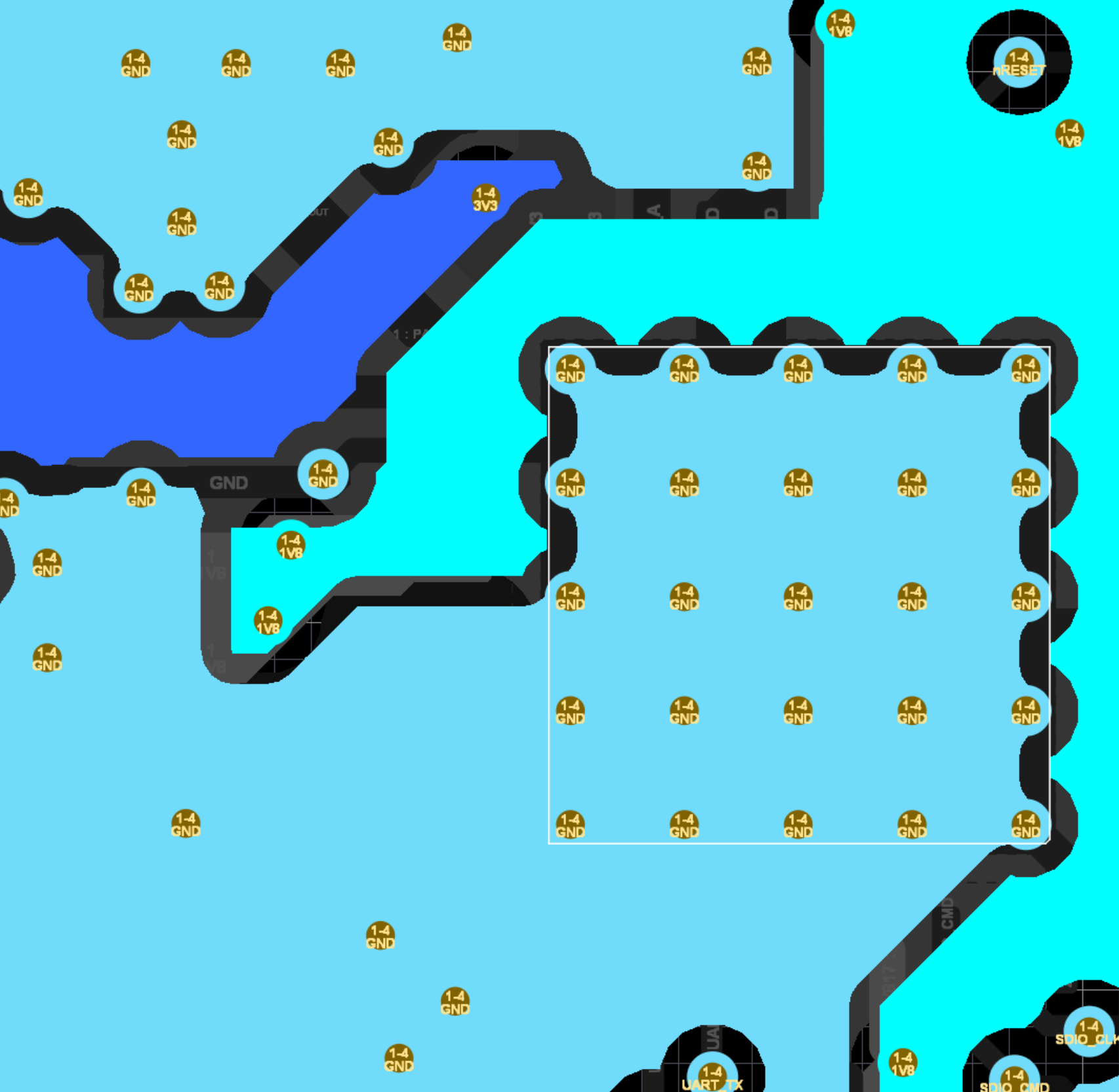
- The 1.8V path must be located around the device on a layer that is not the top layer or ground layer (place it on layer 3 or 4). This way the power path cannot interrupt the RF trace on top layer (layer 1) or the continuous ground layer (layer 2). Only one via is used for each 1.8V power supply, the 1.8V supply currents must not flow under the device.
- For the 3.3V power delivery, a thick trace or a power plane must be used to carry the required amount of current consumption of the PA_LDO_IN. For more information, see Table 2-2. The power delivery must also be placed on a layer that is not top layer or ground layer (layer 3 or 4).
- PA_LDO_IN (pins 39 and 40): These two pins must be shorted together with a solid region. The decoupling capacitor should be placed close to the device. Use two vias if possible to deliver the 3.3V rail.
- The ground for pin 37 and 38 must be shorted together with a solid region. This solid region should be connected to the IC thermal ground pad.
- The ground for pin 3 must be shorted to the thermal pad under the IC and to the ground plane that is adjacent to the RF trace.
Figure 3-13 is sampled from the BP-CC3301 design files.
 Figure 3-13 Reference Layout of CC33xx
Power Supplies
Figure 3-13 Reference Layout of CC33xx
Power SuppliesFigure 3-14 is sampled from the M2-CC3301 design files.
 Figure 3-14 Reference Layout of the Power
Layer