SBAU374A May 2021 – May 2022 DAC12DL3200
- Abstract
- Trademarks
- 1Introduction
- 2Equipment
-
3Setup Procedure
- 3.1 Install the High Speed Data Converter (HSDC) Pro Software
- 3.2 Install the Configuration GUI Software
- 3.3 Connect the DAC12DL3200EVM and TSW14DL3200EVM
- 3.4 Connect the Power Supplies to the Boards (Power Off)
- 3.5 Connect the Signal Generators to the EVM (*RF Outputs Disabled Until Directed)
- 3.6 Turn On the TSW14DL3200EVM 12-V Power and Connect to the PC
- 3.7 Turn On the DAC12DL3200EVM 5-V Power Supply and Connect to the PC
- 3.8 Turn On the Signal Generator RF Outputs
- 3.9 Open the DAC12DL3200EVM GUI and Program the DAC and Clocks for Single Channel, NRZ Mode 2 Operation
- 3.10 Open the HSDC Software and Load the FPGA Image to the TSW14DL3200EVM
- 3.11 DxSTRB Timing Adjustment
- 4Other Modes of Operation
- 5Register Log File
- 6Device Configuration
- A Troubleshooting the DAC12DL3200EVM
- B DAC12DL3200EVM Onboard Clocking Configuration
1.1 Low Latency Evaluation of Receive and Transmit
The TSW14DL3200EVM is designed for plug-and-play evaluation with the DAC12DL3200EVM and ADC12DL3200EVM. This provides a capability for prototyping or testing a low-latency LVDS-based DAC transmitter or ADC receiver, or both simultaneously.
TI takes two approaches for measuring the overall end-to-end latency of the DAC12DL3200 device.
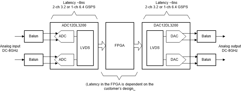
Approach 1: Figure 1-2 illustrates this approach where the test signal is fed into the front end of the ADC12DL3200 device and the samples are extracted and collected by the FPGA. These samples are then forwarded to the DAC12DL3200 which generates the resultant output signal (delayed version of the input test signal). The IO architecture of the Xilinx UltraScale enables extremely high-speed data rates by trading off latency for throughput. At bit-rates over 1.2Gbps, the SERDES blocks in the FPGA implement asynchronous clock domain crossing (both at the ADC and the DAC side). In addition, there is a possibility of bit-slips between data lanes of the ADC and the outputs of the receiving SERDES blocks in the FPGA. These are compensated for with an additional layer of buffering inside the FPGA. The total sum of all of these domain crossing and data-ordering-related delays result in an end-to-end latency of 285 ns. Of this, the DAC12DL3200 contributes approximately 6 ns of latency (see the data sheet spec), while the ADC12DL3200 adds a latency of approximately 8 ns. The remaining delay is from the FPGA logic used.
 Figure 1-2 Low Latency LVDS-Based ADC
Receiver and DAC Transmitter
Figure 1-2 Low Latency LVDS-Based ADC
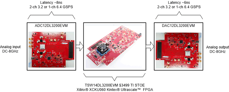
Receiver and DAC TransmitterApproach 2: To minimize the delay through the FPGA and obtain a true representation of the latency of the data converters, a simplified setup is created, where the FPGA is used as a combinatorial pass-through device. The FPGA logic passes just the MSB output of the ADC (through the FPGA) to the MSB input of the DAC. The FPGA does not carry out any re-timing of the signals to avoid any non-deterministic delays on account of clock domain crossing. Using this setup, the measured combined latency of ADC12DL3200 + FPGA + DAC12DL3200 + Device EVM routing is 32.8 ns .
 Figure 1-3 Low Latency ADC EVM, Capture
Card and Pattern Generator, and DAC EVM