SBAU436A January   2024  – February 2024


  1.   1
  2.   Description
  3.   Get Started
  4.   Features
  5.   Applications
  6.   6
  7. 1Evaluation Module Overview
    1. 1.1 Introduction
    2. 1.2 Kit Contents
    3. 1.3 Specification
    4. 1.4 Device Information
  8. 2Hardware
    1. 2.1 EVM Analog Input Options
      1. 2.1.1 Differential SMA Inputs
      2. 2.1.2 Single-Ended SMA Inputs
      3. 2.1.3 Differential Input Pins
    2. 2.2 Power Supplies
    3. 2.3 ADC Connections and Decoupling
    4. 2.4 ADC Input Amplifiers
    5. 2.5 VCOM Buffer
    6. 2.6 Voltage Reference
    7. 2.7 Clock Tree
    8. 2.8 Digital Interfaces
  9. 3Software
    1. 3.1 ADS1278EVM Software Installation
  10. 4Implementation Results
    1. 4.1 Hardware Connections
    2. 4.2 Optional EVM Configuration
    3. 4.3 GUI Settings for ADC Control
    4. 4.4 Time Domain Display
    5. 4.5 Frequency Domain Display
    6. 4.6 Histogram Display
  11. 5Hardware Design Files
    1. 5.1 Schematics
    2. 5.2 PCB Layouts
    3. 5.3 Bill of Materials (BOM)
  12. 6Additional Information
    1. 6.1 Trademarks
  13. 7References
  14. 8Revision History

PCB Layouts

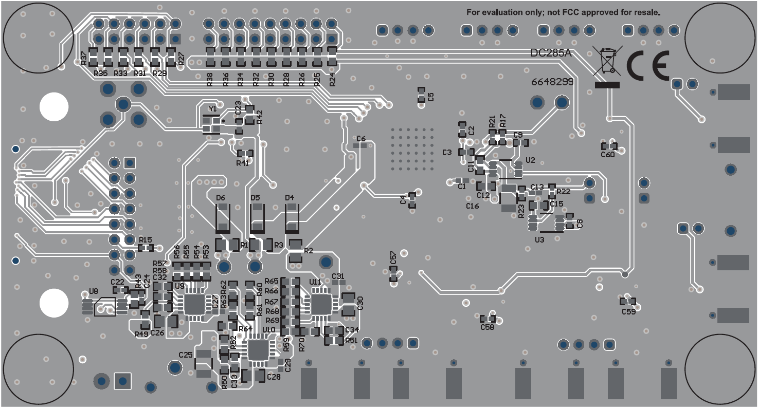
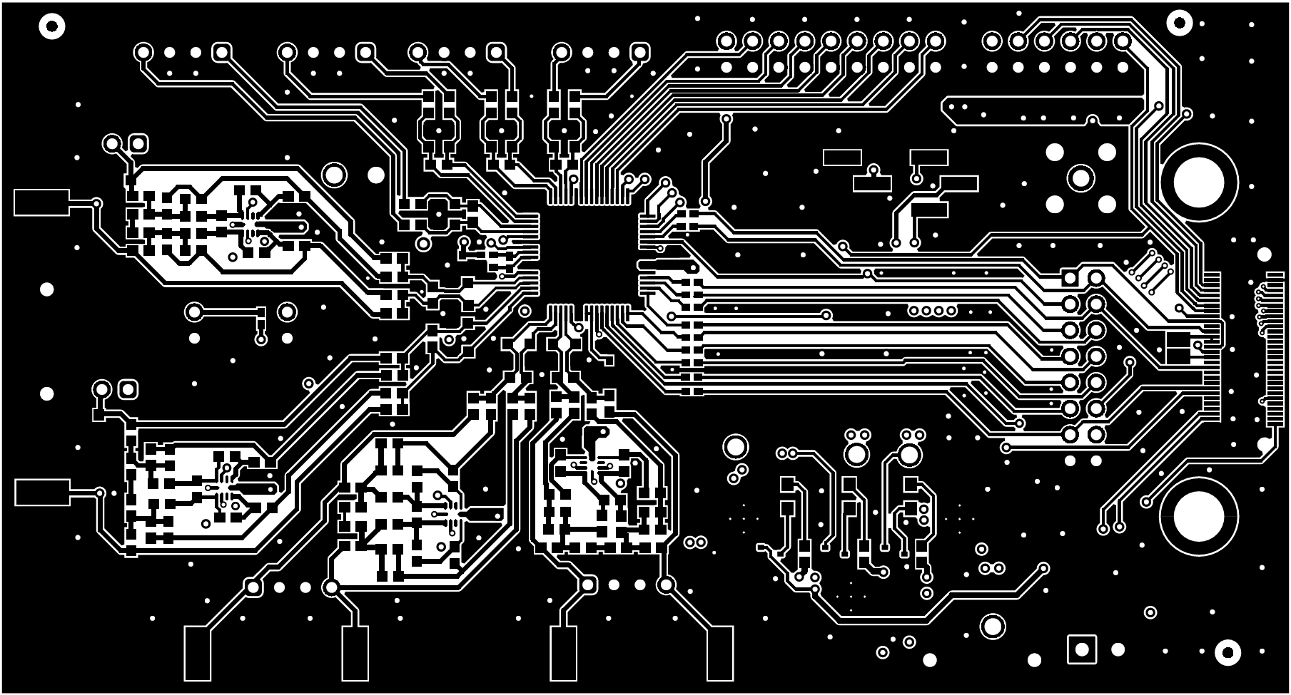
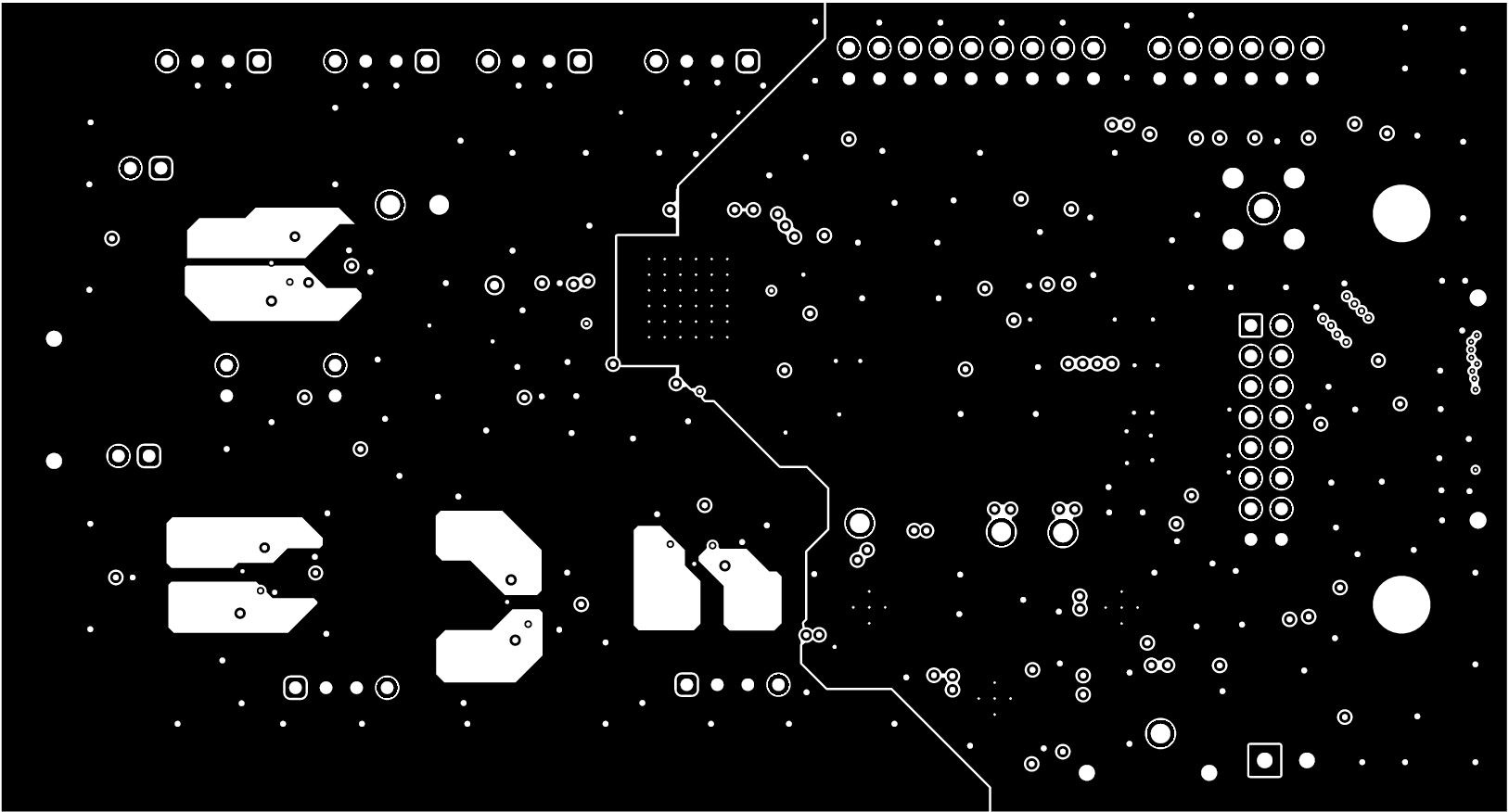
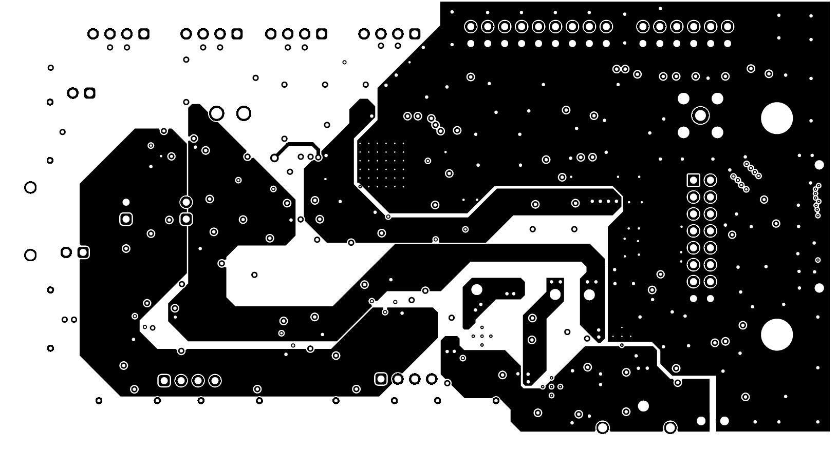
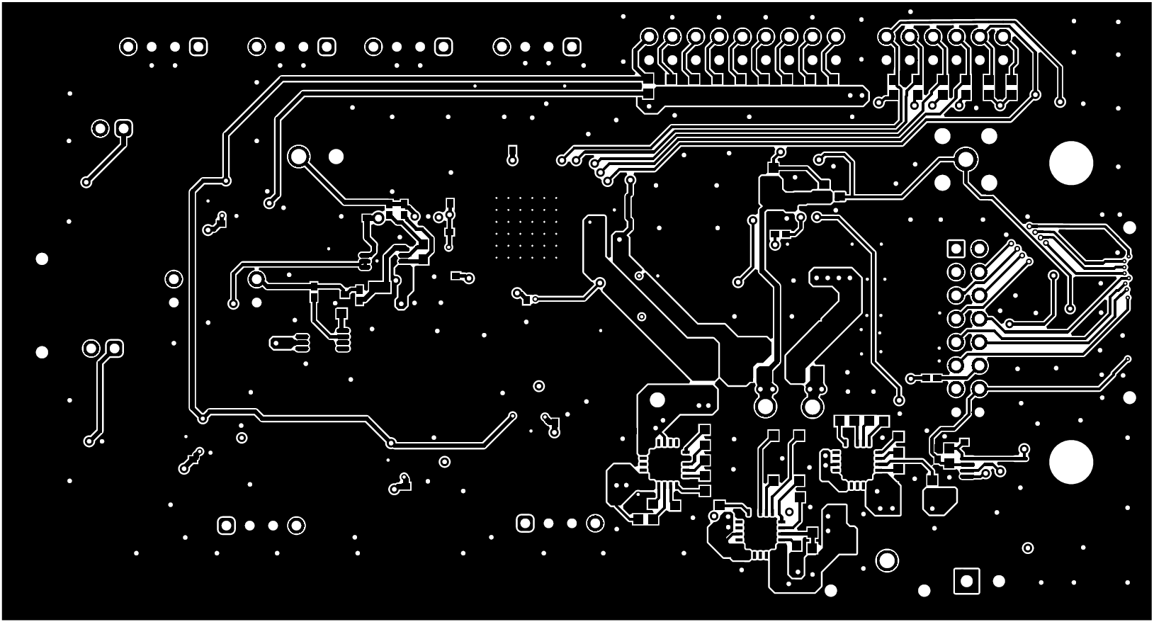
Figure 6-6 through Figure 6-11 show the PCB layouts for the ADS1278 EVM.
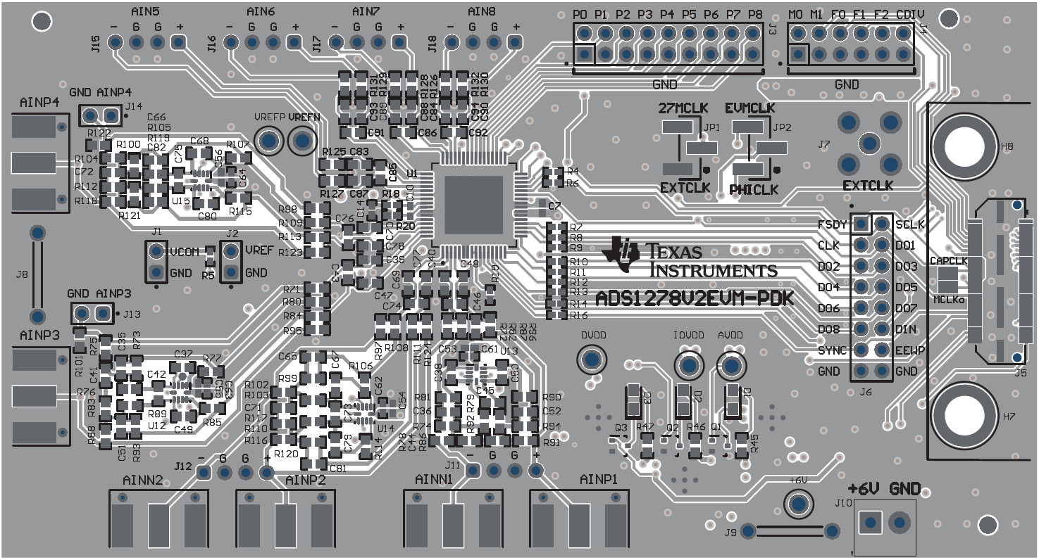
GUID-20231113-SS0I-R0H5-6M3S-94WPFDWW10H9-low.pngFigure 5-6 Top Side Composite Layout
GUID-20231113-SS0I-FXVQ-9HSN-HXLLGJZTWLQX-low.pngFigure 5-7 Bottom Side Composite Layout
GUID-20231113-SS0I-7DX8-K5ZW-RT9KRFRGPM1P-low.pngFigure 5-8 Top Signal Layer Layout
GUID-20231113-SS0I-48SM-DF6D-PFDQ08JXFJ8K-low.pngFigure 5-9 Ground Layer Layout
GUID-20231113-SS0I-QZM7-LLXX-NPMQQT9FM8MR-low.pngFigure 5-10 Power Layer Layout
GUID-20231113-SS0I-8NTK-CX3L-7LPRSGNBNH97-low.pngFigure 5-11 Bottom Signal Layer Layout