SBOA221A January 2018 – February 2019 TLV1702 , TLV431
Design Goals
| Input | Output | Supply | ||||
|---|---|---|---|---|---|---|
| ViMin | ViMax | VoMin | VoMax | Vcc | Vee | Vref |
| 0 V | 5 V | 0 V | 36 V | 5 V | 0 V | 2.5 V |
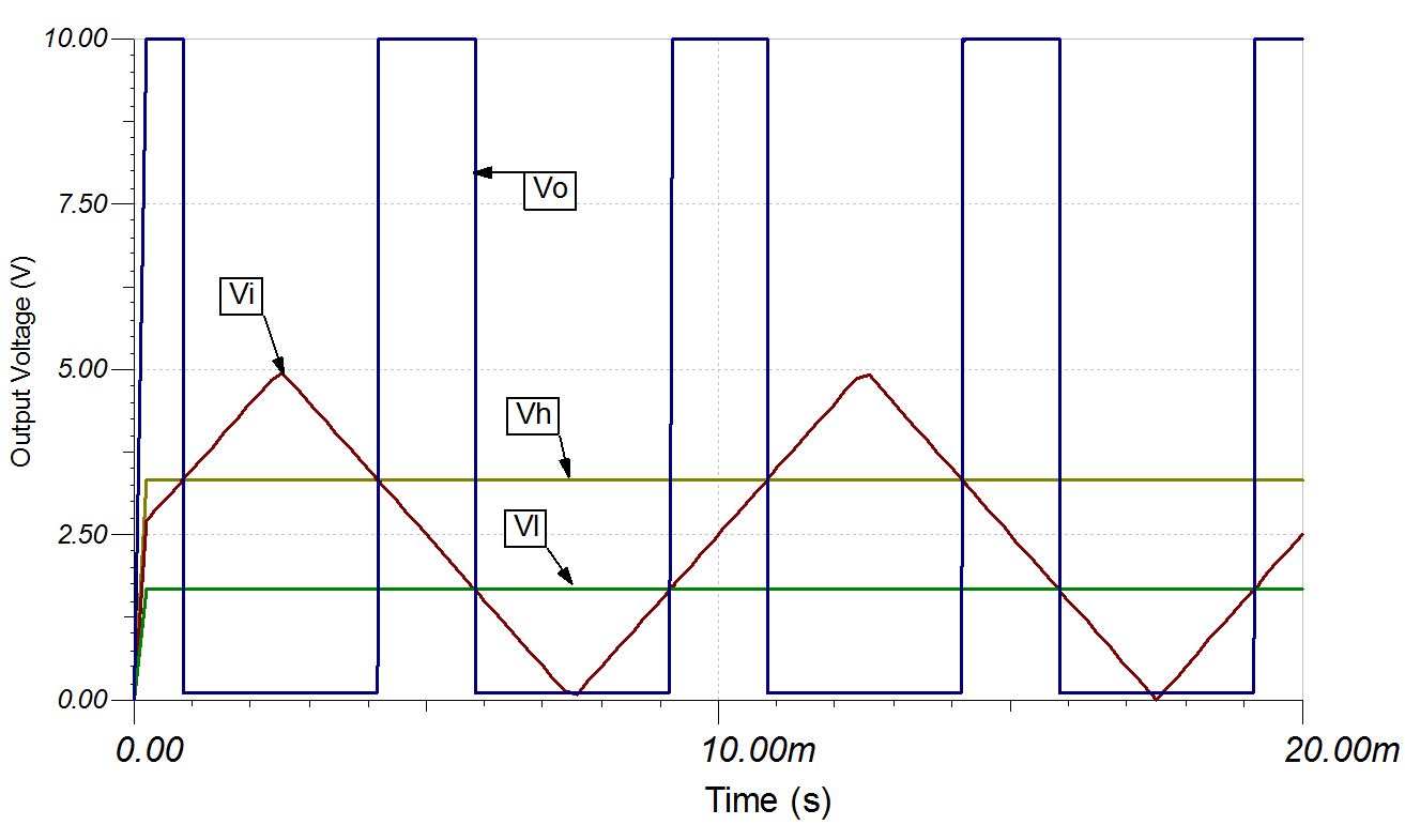
| VL (Lower Threshold) | VH (Upper Threshold) | Upper to Lower Threshold Ratio |
|---|---|---|
| 1.66 V | 3.33 V | 2 |
Design Description
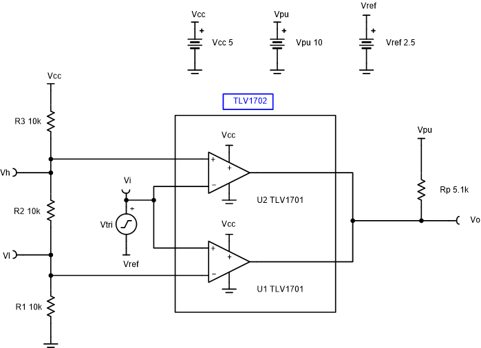
This circuit utilizes two comparators in parallel to determine if a signal is between two reference voltages. If the signal is within the window, the output is high. If the signal level is outside of the window, the output is low. For this design, the reference voltages are generated from a single supply with voltage dividers.
Design Notes
- The input should not exceed the common mode limitations of the comparators.
- If higher pullup voltages are used, Rp should be sized accordingly to prevent large current draw. The TLV1701 supports pullup voltages up to 36 V.
- Comparator must be open-drain or open-collector to allow for the ORed output.
Design Steps
- Define the upper (VH)
and lower (VL) window voltages.
- Choose resistor values to achieve
the desired window voltages.
Design Simulations
Transient Simulation Results
Design References
See Analog Engineer's Circuit Cookbooks for TI's comprehensive circuit library.
See the circuit SPICE simulation file SBOC516.
See TIPD178.
Design Featured Op Amp
| TLV1702 | |
|---|---|
| Vcc | 2.2 V to 36 V |
| VinCM | Rail-to-rail |
| Vout | Open Collector (36 V Maximum) |
| Vos | 2.5 mV |
| Iq | 75 µA/Ch |
| Ib | 15 nA |
| Rise Time | 365 ns |
| Fall Time | 240 ns |
| #Channels | 1, 2, and 4 |
| TLV1702 | |