SLAU472C February 2013 – November 2023 TAS2505 , TAS2505-Q1
- 1
- Trademarks
- 1 TAS2505 Device Overview
- 2Description
-
3
TAS2505 Application
- 3.1 Terminal Descriptions
- 3.2 Audio Analog I/O
- 3.3 Analog Signals
- 3.4
Audio DAC and Audio Analog Outputs
- 3.4.1 DAC
- 3.4.2 DAC Gain Setting
- 3.4.3 Interrupts
- 3.4.4 Programming DAC Digital Filter Coefficients
- 3.4.5 Updating DAC Digital Filter Coefficients During PLAY
- 3.4.6 Digital Mixing and Routing
- 3.4.7 Analog Audio Routing
- 3.4.8 Analog Outputs
- 3.4.9 Audio Output-Stage Power Configurations
- 3.4.10 5V LDO
- 3.4.11 POR
- 3.4.12 DAC Setup
- 3.5
PowerTune
- 3.5.1 PowerTune Modes
- 3.5.2 DAC Power Consumption
- 3.5.3
Speaker output Power Consumption
- 3.5.3.1 Speaker output, Mono, 48 kHz, Highest Performance, DVDD = IOVDD = 1.8 V, AVDD = 1.8 V, SPKVDD = 3.6V
- 3.5.3.2 Speaker output, Mono, Lowest Power Consumption
- 3.5.3.3 Speaker output, Mono, 8 kHz, Highest Performance, DVDD = IOVDD = 1.8 V, AVDD = 1.8 V, SPKVDD = 3.6V
- 3.5.3.4 Speaker output, Mono, Lowest Power Consumption
- 3.5.4
Headphone output Power Consumption
- 3.5.4.1 Headphone output, Mono, 48 kHz, Highest Performance, DVDD = IOVDD = 1.8 V, AVDD = 1.8 V, SPKVDD = 3.6V
- 3.5.4.2 Headphone output, Mono, Lowest Power Consumption, DVDD = IOVDD = 1.8 V, AVDD = 1.5 V, SPKVDD = 3.6V
- 3.5.4.3 Headphone output, Mono, 8 kHz, Highest Performance, DVDD = IOVDD = 1.8 V, AVDD = 1.8 V, SPKVDD = 3.6V
- 3.5.4.4 Headphone output, Mono, Lowest Power Consumption, DVDD = IOVDD = 1.8 V, AVDD = 1.8 V, SPKVDD = 3.6V
- 3.6 CLOCK Generation and PLL
- 3.7 Digital Audio and Control Interface
- 3.8 Power Supply
- 3.9 Device Special Functions
- 4Device Initialization
-
5Example Setups
- 5.1 Example Register Setup to Play Digital Data Through DAC and Headphone/Speaker Outputs
- 5.2 Example Register Setup to Play Digital Data Through DAC and Headphone Output
- 5.3 Example Register Setup to Play AINL and AINR Through Headphone/Speaker Outputs
- 5.4 Example Register Setup to Play AINL and AINR Through Headphone Output
- 5.5 Example Register Setup to Play Digital Data Through DAC and Headphone/Speaker Outputs With 3 Programmable Biquads
- 5.6 Example Register Setup to Play Digital Data Through DAC and Headphone/Speaker Outputs With 6 Programmable Biquads
-
6Register Map
- 6.1
TAS2505 Register Map
- 6.1.1 Control Registers, Page 0 (Default Page): Clock Multipliers, Dividers, Serial Interfaces, Flags, Interrupts, and GPIOs
- 6.1.2 Control Registers, Page 1: DAC Routing, Power-Controls and MISC Logic Related Programmabilities
- 6.1.3 Page 2 - 43: Reserved Register
- 6.1.4 Page 44: DAC Programmable Coefficients RAM
- 6.1.5 Page 45 - 52: DAC Programmable Coefficients RAM
- 6.1.6 Page 53 - 61: Reserved Register
- 6.1.7 Page 62 - 70: DAC Programmable Coefficients RAM
- 6.1.8 Pages 71 – 255: Reserved Register
- 6.1.9 DAC Coefficients A+B
- 6.1.10 DAC Defaults
- 6.1
TAS2505 Register Map
- 7Revision History
3.4.1.3.2 Biquad Section
The transfer function of each of the biquad filters is given by
Equation 2. 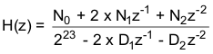
Table 3-6 DAC Biquad Filter Coefficients
| Filter | Coefficient | Mono DAC Channel | Default (Reset) Values |
|---|---|---|---|
| Biquad A | N0 | C1 (Page 44, registers 12, 13, 14) | 0x7FFFFF |
| N1 | C2 (Page 44, registers 16, 17, 18) | 0x000000 | |
| N2 | C3 (Page 44, registers 20, 21, 22) | 0x000000 | |
| D1 | C4 (Page 44, registers 24, 25, 26) | 0x000000 | |
| D2 | C5 (Page 44, registers 28, 29, 30) | 0x000000 | |
| Biquad B | N0 | C6( Page 44, registers 32, 33, 34) | 0x7FFFFF |
| N1 | C7 (Page 44, registers 36, 37, 38) | 0x000000 | |
| N2 | C8 (Page 44, registers 40, 41, 42) | 0x000000 | |
| D1 | C9 (Page 44, registers 44, 45, 46) | 0x000000 | |
| D2 | C10 (Page 44, registers 48, 49, 50) | 0x000000 | |
| Biquad C | N0 | C11 (Page 44, registers 52, 53, 54) | 0x7FFFFF |
| N1 | C12 (Page 44, registers 56, 57, 58) | 0x000000 | |
| N2 | C13 (Page 44, registers 60, 61, 62) | 0x000000 | |
| D1 | C14 (Page 44, registers 64, 65, 66) | 0x000000 | |
| D2 | C15 (Page 44, registers 68, 69, 70) | 0x000000 | |
| Biquad D | N0 | C16 (Page 44, registers 72, 73, 74) | 0x7FFFFF |
| N1 | C17 (Page 44, registers 76, 77, 78) | 0x000000 | |
| N2 | C18 (Page 44, registers 80, 81, 82) | 0x000000 | |
| D1 | C19 (Page 44, registers 84, 85, 86) | 0x000000 | |
| D2 | C20 (Page 44, registers 88, 89, 90) | 0x000000 | |
| Biquad E | N0 | C21 (Page 44, registers 92, 93, 94) | 0x7FFFFF |
| N1 | C22 (Page 44, registers 96, 97, 98) | 0x000000 | |
| N2 | C23 (Page 44, registers 100, 101, 102) | 0x000000 | |
| D1 | C24 (Page 44, registers 104, 105, 106) | 0x000000 | |
| D2 | C25 (Page 44, registers 108, 109, 110) | 0x000000 | |
| Biquad F | N0 | C26 (Page 44, registers 112, 113, 114) | 0x7FFFFF |
| N1 | C27 (Page 44, registers 116, 117, 118) | 0x000000 | |
| N2 | C28 (Page 44, registers 120, 121, 122) | 0x000000 | |
| D1 | C29 (Page 44, registers 124, 125, 126) | 0x000000 | |
| D2 | C30 (Page 45, registers 8, 9, 10) | 0x000000 |