SLAU472C February 2013 – November 2023 TAS2505 , TAS2505-Q1
- 1
- Trademarks
- 1 TAS2505 Device Overview
- 2Description
-
3
TAS2505 Application
- 3.1 Terminal Descriptions
- 3.2 Audio Analog I/O
- 3.3 Analog Signals
- 3.4
Audio DAC and Audio Analog Outputs
- 3.4.1 DAC
- 3.4.2 DAC Gain Setting
- 3.4.3 Interrupts
- 3.4.4 Programming DAC Digital Filter Coefficients
- 3.4.5 Updating DAC Digital Filter Coefficients During PLAY
- 3.4.6 Digital Mixing and Routing
- 3.4.7 Analog Audio Routing
- 3.4.8 Analog Outputs
- 3.4.9 Audio Output-Stage Power Configurations
- 3.4.10 5V LDO
- 3.4.11 POR
- 3.4.12 DAC Setup
- 3.5
PowerTune
- 3.5.1 PowerTune Modes
- 3.5.2 DAC Power Consumption
- 3.5.3
Speaker output Power Consumption
- 3.5.3.1 Speaker output, Mono, 48 kHz, Highest Performance, DVDD = IOVDD = 1.8 V, AVDD = 1.8 V, SPKVDD = 3.6V
- 3.5.3.2 Speaker output, Mono, Lowest Power Consumption
- 3.5.3.3 Speaker output, Mono, 8 kHz, Highest Performance, DVDD = IOVDD = 1.8 V, AVDD = 1.8 V, SPKVDD = 3.6V
- 3.5.3.4 Speaker output, Mono, Lowest Power Consumption
- 3.5.4
Headphone output Power Consumption
- 3.5.4.1 Headphone output, Mono, 48 kHz, Highest Performance, DVDD = IOVDD = 1.8 V, AVDD = 1.8 V, SPKVDD = 3.6V
- 3.5.4.2 Headphone output, Mono, Lowest Power Consumption, DVDD = IOVDD = 1.8 V, AVDD = 1.5 V, SPKVDD = 3.6V
- 3.5.4.3 Headphone output, Mono, 8 kHz, Highest Performance, DVDD = IOVDD = 1.8 V, AVDD = 1.8 V, SPKVDD = 3.6V
- 3.5.4.4 Headphone output, Mono, Lowest Power Consumption, DVDD = IOVDD = 1.8 V, AVDD = 1.8 V, SPKVDD = 3.6V
- 3.6 CLOCK Generation and PLL
- 3.7 Digital Audio and Control Interface
- 3.8 Power Supply
- 3.9 Device Special Functions
- 4Device Initialization
-
5Example Setups
- 5.1 Example Register Setup to Play Digital Data Through DAC and Headphone/Speaker Outputs
- 5.2 Example Register Setup to Play Digital Data Through DAC and Headphone Output
- 5.3 Example Register Setup to Play AINL and AINR Through Headphone/Speaker Outputs
- 5.4 Example Register Setup to Play AINL and AINR Through Headphone Output
- 5.5 Example Register Setup to Play Digital Data Through DAC and Headphone/Speaker Outputs With 3 Programmable Biquads
- 5.6 Example Register Setup to Play Digital Data Through DAC and Headphone/Speaker Outputs With 6 Programmable Biquads
-
6Register Map
- 6.1
TAS2505 Register Map
- 6.1.1 Control Registers, Page 0 (Default Page): Clock Multipliers, Dividers, Serial Interfaces, Flags, Interrupts, and GPIOs
- 6.1.2 Control Registers, Page 1: DAC Routing, Power-Controls and MISC Logic Related Programmabilities
- 6.1.3 Page 2 - 43: Reserved Register
- 6.1.4 Page 44: DAC Programmable Coefficients RAM
- 6.1.5 Page 45 - 52: DAC Programmable Coefficients RAM
- 6.1.6 Page 53 - 61: Reserved Register
- 6.1.7 Page 62 - 70: DAC Programmable Coefficients RAM
- 6.1.8 Pages 71 – 255: Reserved Register
- 6.1.9 DAC Coefficients A+B
- 6.1.10 DAC Defaults
- 6.1
TAS2505 Register Map
- 7Revision History
3.6.1 PLL
For lower power consumption, it is best to derive the internal audio processing clocks using the simple dividers. When the input MCLK or other source clock is not an integer multiple of the audio processing clocks, then it is necessary to use the on-board PLL. The TAS2505 fractional PLL can be used to generate an internal master clock used to produce the processing clocks needed by the DAC and Digital Effects. The programmability of this PLL allows operation from a wide variety of clocks that may be available in the system.
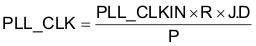
The PLL input supports clocks varying from 512 kHz to 20 MHz and is register programmable to enable generation of required sampling rates with fine resolution. The PLL can be turned on by writing to page 0 / register 5, bit D7. When the PLL is enabled, the PLL output clock PLL_CLK is given by the following equation:
where
R = 1, 2, 3, ..., 16 (page 0 / register 5, default value = 1)
J = 1, 2, 3, …, 63, (page 0 / register 6, default value = 4)
D = 0, 1, 2, …, 9999 (page 0 / register 7 and 8, default value = 0)
P = 1, 2, 3, …, 8 (page 0 / register 5, default value = 1)
The PLL can be turned on via page 0, register 5, bit D7. The variable P can be programmed via page 0, register 5, bits D6–D4. The variable R can be programmed via page 0, register 5, bits D3–D0. The variable J can be programmed via page 0, register 6, bits D5–D0. The variable D is 14 bits and is programmed into two registers. The MSB portion can be programmed via page 0, register 7, bits D5–D0, and the LSB portion is programmed via page 0, register 8, bits D7–D0. For proper update of the D-divider value, page 0, register 7 must be programmed first, followed immediately by page 0, register 8. Unless the write to page 0, register 8 is completed, the new value of D does not take effect.
When the PLL is enabled, the following conditions must be satisfied.
- When the PLL is enabled and D = 0, the following conditions must be satisfied for PLL_CLKIN: Equation 8.
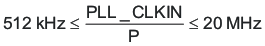
80 MHz ≤ (PLL_CLKIN × J.D × R/P) ≤ 110 MHz
Equation 9. 4 ≤ R × J ≤ 259 - When the PLL is enabled and D ≠ 0, the following conditions must be satisfied for PLL_CLKIN: Equation 10.
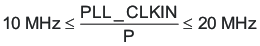 Equation 11. 80 MHz ≤ (PLL_CLKIN × J.D × R/P) ≤ 110 MHzEquation 12. R = 1