SLUAAP4 October 2023 LM2005 , LM2101 , LM2103 , LM2104 , LM2105 , LM5108 , UCC27531 , UCC27710 , UCC44273
5 Board Space, Thermal Performance, and Other Considerations
The primary way that gate drivers can help to reduce board space is with their packages.
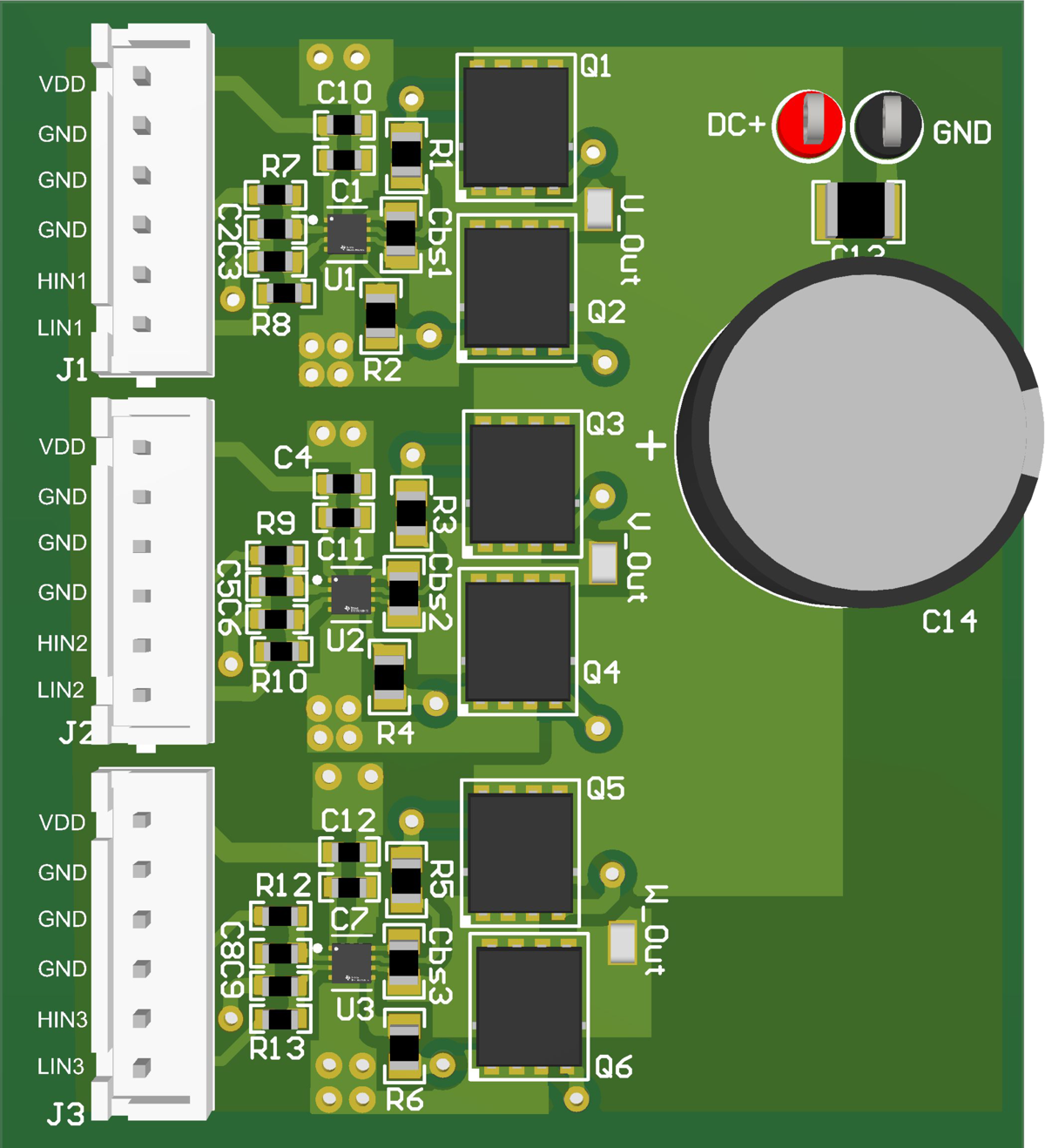
For example, consider a three-phase BLDC motor drive configuration. When using a driver in a large package, evenly spacing the driver IC relative to the three power switches can be difficult, leaving one of the signals out of phase. A compact half-bridge driver helps to minimizes the space between the driver and the power switch. Minimizing the PCB traces between the driver and switch helps to reduce parasitics from layout. Figure 5-1 shows an example BLDC layout using the LM2105 in the 2 mm x 2 mm WSON package option, LM2105DSGR (U1, U2 and U3).

Figure 5-1 A BLDC Motor Drive PCB Layout Example Using Three LM2105DSGR Half-Bridge Drivers.
Select features of gate drivers can also eliminate the need for external circuitry, further reducing the number of components and, in turn, overall size. For example, integrated negative voltage tolerance and reverse current handling in a device like UCC27624 help to eliminate clamp diodes on the driver inputs and outputs.
Half-bridge designs often utilize a bootstrap circuit consisting of a capacitor, resistor, and diode. Another way to save on board space is to choose a half-bridge driver that integrates the bootstrap diode (and resistor) within the driver. With such a driver, the only bootstrap element required on the board is the capacitor.
Applications like stepper motor drives often require many signals from the microcontroller. So, there is an additional focus on minimizing the number of PWM inputs required by the gate driver. In these cases, look for gate drivers that offer a single-PWM compatibility, which is often implemented in one of two ways:
- One input pin (PWM or IN, or named like a high-side input HI or INH). This is paired with a second, optional input (like EN or SD for enable or shutdown functionality). See example using half-bridge driver LM2104 in Figure 5-2.
A high-side input pin (HI or INH) paired with an inverted low-side input (nLI or nINL). See example implementation using half-bridge driver LM2103 in Figure 5-2.
 Figure 5-2 Examples of Different Input Configurations Using LM2103, LM2104
Gate drivers can especially help reduce size when multiple of these elements are combined. For example, LM2105 (105-V, 0.5-A/0.8-A half-bridge driver) has an integrated bootstrap diode and -18-V negative transient voltage capability (on VHS)—all within a 2-mm by 2-mm WSON package (TI package name “DSG”).
In addition to board space savings, a small package like DSG package can offer thermal benefits. For example, in a BLDC system, using three half-bridge drivers in compact packages allows each driver to dissipate power individually (as opposed to dissipating through one larger package for all three phases). The DSG package also includes a thermal pad to help dissipate additional power and further improve thermal efficiency.
To quantify this improvement in thermal performance, this example compares the SOIC (“D”) and WSON (“DSG”) packages of LM2105. The maximum power dissipation in the gate driver (PMAX) can be calculated using the junction and ambient temperatures in addition to the junction-to-ambient thermal resistance (RϴJA) as specified in the Thermal Information section of the device’s data sheet:
For the same junction temperature (TJ) and ambient temperature (TA), the maximum power dissipation for each variant of LM2105 is inversely proportional to RϴJA. The RϴJA for the D-package version is approximately 1.7 times larger than that of the DSG-package version (133.2 versus 78.2). So, the DSG-package version can, at maximum, dissipate 1.7 times more power than the SOIC-package version under the same temperature conditions. For more information about thermal metrics, refer to the application note Semiconductor and IC Package Thermal Metrics.