SLUUCN1C June 2022 – December 2022 UCC28C50 , UCC28C50-Q1 , UCC28C51 , UCC28C51-Q1 , UCC28C52 , UCC28C52-Q1 , UCC28C53 , UCC28C53-Q1 , UCC28C54 , UCC28C54-Q1 , UCC28C55 , UCC28C55-Q1 , UCC28C56H , UCC28C56H-Q1 , UCC28C56L , UCC28C56L-Q1 , UCC28C57H , UCC28C57H-Q1 , UCC28C57L , UCC28C57L-Q1 , UCC28C58 , UCC28C58-Q1 , UCC28C59 , UCC28C59-Q1
- Trademarks
- 1General Texas Instruments High Voltage Evaluation (TI HV EVM) User Safety Guidelines
- 2Description
- 3Schematic Diagram
- 4EVM Setup and Operation
-
5Performance Data
- 5.1 Efficiency Versus Load, 10% to 100% Load
- 5.2 Efficiency Versus VIN at 100% Load
- 5.3 Power Loss Versus Load, 10% to 100% Load
- 5.4 Load Regulation, 10% to 100% Load
- 5.5 Light Load Regulation, 0-mA to 200-mA Load
- 5.6 Line Regulation, Various Loads
- 5.7 Startup Waveforms
- 5.8 Shutdown Waveforms
- 5.9 Output Voltage Ripple
- 5.10 Steady State Switching Waveforms
- 5.11 Transient Load Waveforms
- 5.12 Over Current and Short Circuit Protections
- 5.13 Stability Measurements
- 5.14 Thermal Measurements
- 6Assembly and Printed Circuit Board (PCB)
- 7Bill of Materials (BOM)
- 8Revision History
6 Assembly and Printed Circuit Board (PCB)
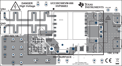
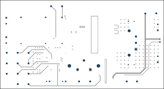
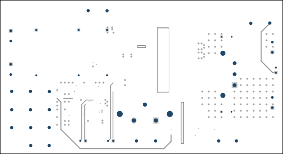
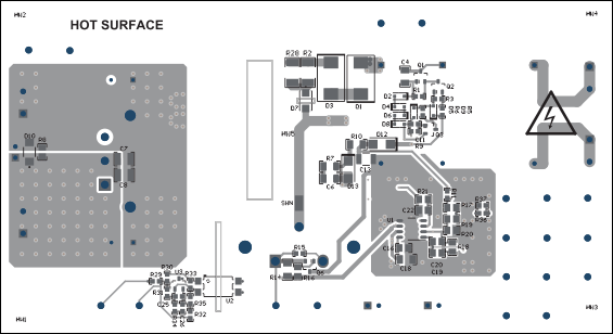
The UCC28C56EVM-066 is designed using a four-layer PCB. Only traces on the top and bottom layers are used for UCC28C56 connections, so the EVM is basically a two-layer PCB. The two middle layers are dedicated to routing only the test points.
 Figure 6-1 UCC28C56EVM-066, PCB Top
Layer, Assembly
 Figure 6-2 UCC28C56EVM-066, Signal
Layer 1, Routing for test points only
 Figure 6-3 UCC28C56EVM-066, Signal
Layer 2, Routing for test points only
 Figure 6-4 UCC28C56EVM-066, PCB
Bottom Layer, Assembly (mirrored view)