SLVAFI8 February 2023 TLC6C5748-Q1
- Abstract
- Trademarks
- 1Introduction
-
2Design Considerations for Low EMI
- 2.1 Design Considerations Overview
- 2.2
Considerations in Detail
- 2.2.1 Top-Level Architecture
- 2.2.2
High Frequency Signals
- 2.2.2.1 Original Setup
- 2.2.2.2 3.3 V I/O Voltage Instead of 5 V
- 2.2.2.3 Use Independent OSC for GSCLK With Spread Spectrum
- 2.2.2.4 Without Using Buffer on GSCLK
- 2.2.2.5 Using Snubber on GSCLK
- 2.2.2.6 Lower the Signal Frequency
- 2.2.2.7 Placement and PCB layout
- 2.2.2.8 ESD Enhancement
- 2.2.2.9 Demo and Test Results
- 2.2.2.10 Bench Test Results
- 3Summary
- 4References
2.2.2.7 Placement and PCB layout
As shared previously, R-C or FB-C filters can be used to dump the high frequency harmonics. The recommendation is to place the R-C filters on the system board. Another filter on LED board is also recommended to have more attenuation, and the filter needs to be placed as close as possible to the connectors.
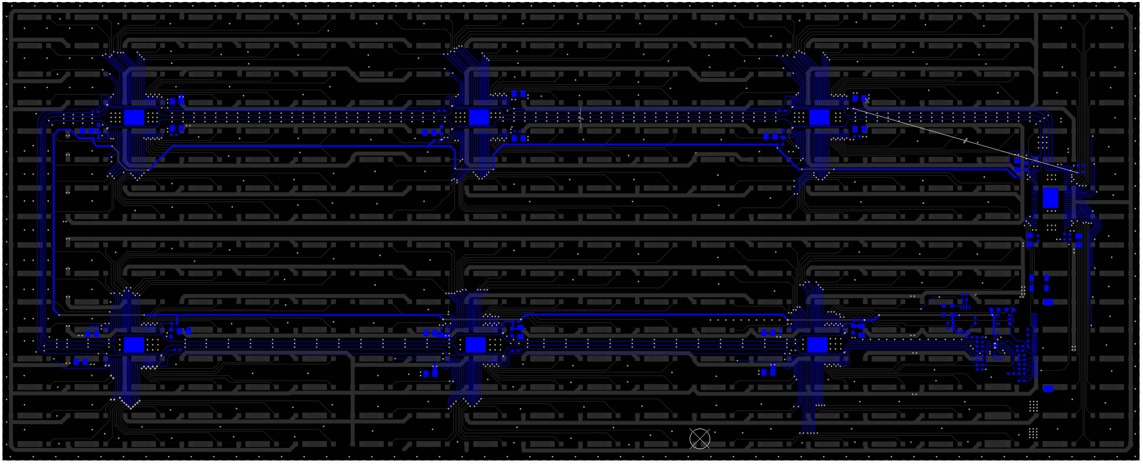
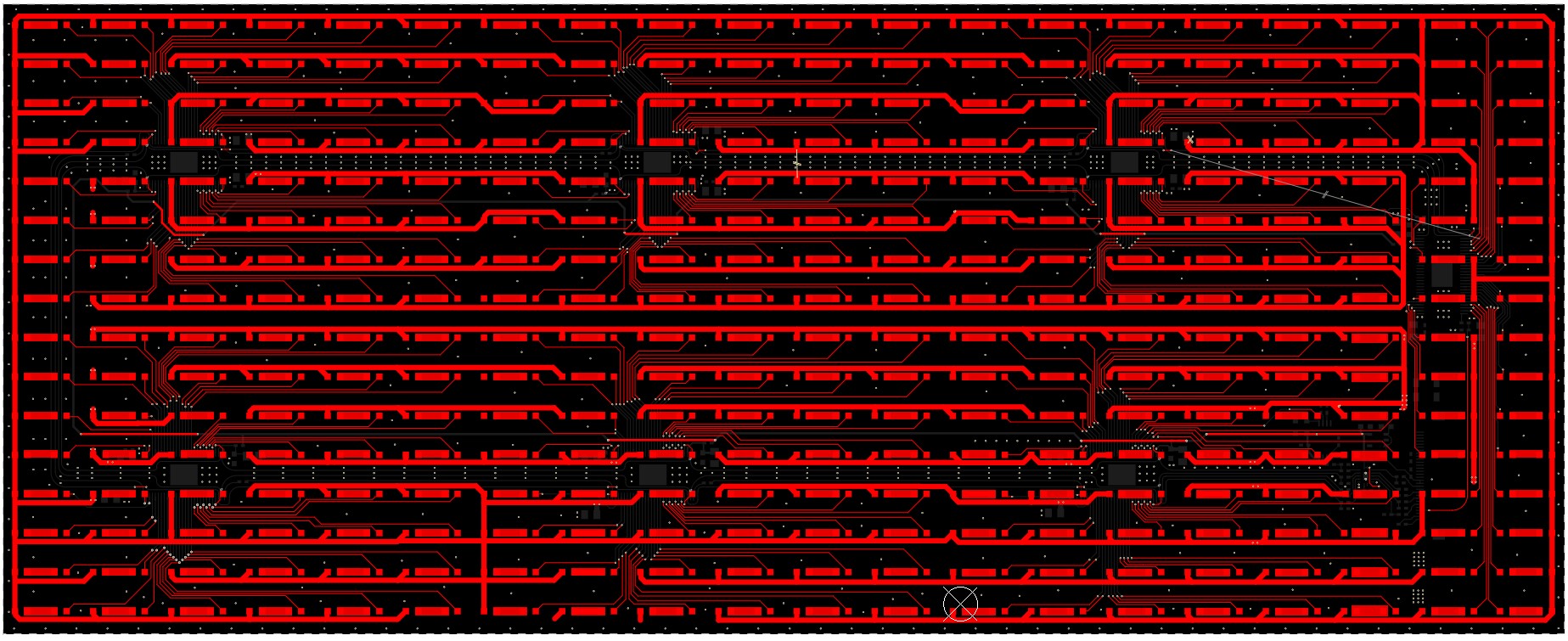
Besides the general PCB layout guidelines on TLC6C5748-Q1, it is also important to provide a low impedance return path for the signal traces. An integrated and continuous GND plane might not be easy for 2-layer PCB board, but it needs to be done as much as possible. For the signal traces, GSCLK, SIN, SCLK should be placed on the bottom layer only. It’s better not to use vias on these traces. While the signal traces are parallel, evenly spaced vias need to be put between them to have the GND plane integrated.
#FIG_Q5X_YW4_FWB shows the reference layout bottom layer (blue) and top layer (red).
 Figure 2-10 Bottom Layer of PCB
Layout
 Figure 2-11 Top layer of PCB
Layout