SLVU179B October   2006  – February 2022 TPS51117


  1.   Trademarks
  2. 1Introduction
    1. 1.1 Description
    2. 1.2 Features
    3. 1.3 Operating Specification
    4. 1.4 Schematic
  3. 2Test Setup
    1. 2.1 Test Equipment
    2. 2.2 Test Points
    3. 2.3 Recommended Test Setup
    4. 2.4 Standard Test Procedures
      1. 2.4.1 Line/Load Regulation
      2. 2.4.2 Output Ripple Measurement
  4. 3Performance Data and Typical Characteristic Curves
  5. 4Board Layout Using TPS51117RGY (QFN 14)
  6. 5List of Materials
  7. 6Revision History

Board Layout Using TPS51117RGY (QFN 14)

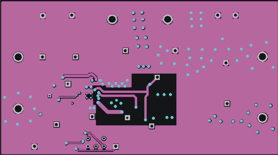
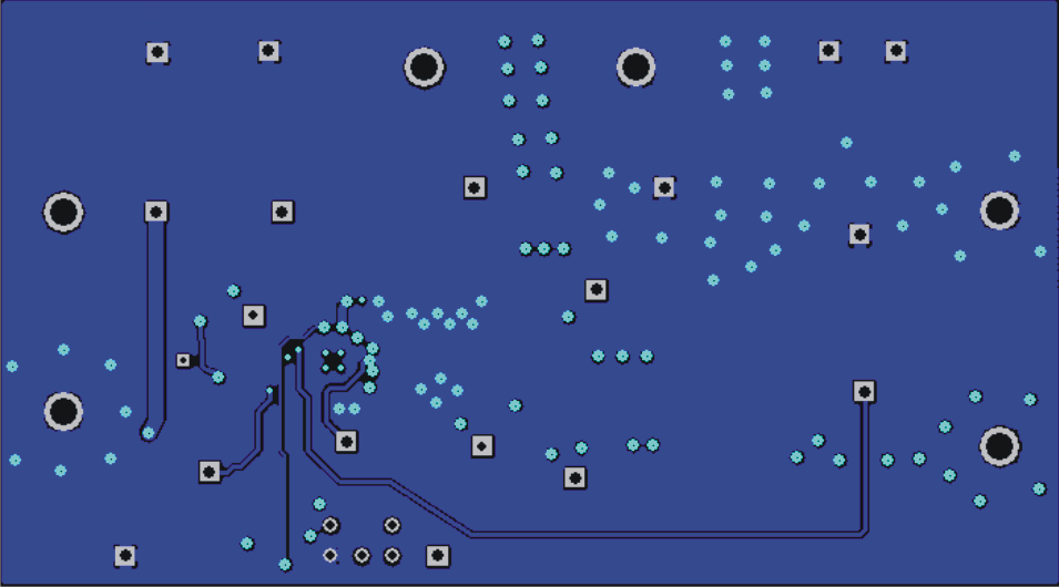
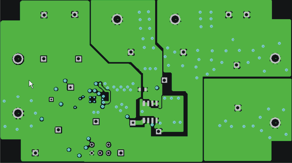
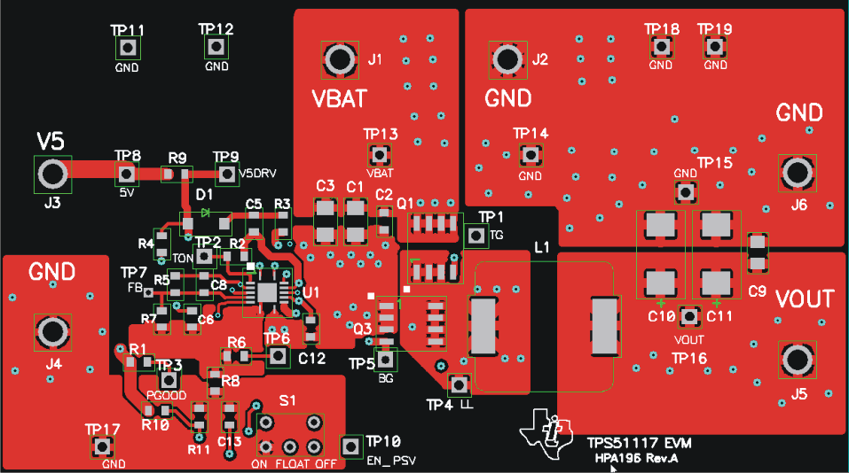
Figure 4-1 through Figure 4-4 show the design of the TPS51117EVM printed circuit board. The EVM has been designed using four layers on a two-ounce copper circuit board.
GUID-6DB298DA-7D84-4005-AD0C-CA1474BF664A-low.gifFigure 4-1 Top Layer Copper
GUID-673CF549-BEC3-43CE-B932-7AC35A9742A8-low.gifFigure 4-2 Layer 2 (Internal 1) Copper
GUID-2B8FFD62-88D6-422C-8942-A9592B03E23E-low.gifFigure 4-3 Layer 3 (Internal 2) Copper
GUID-9DE094AF-E0A5-4D51-BE6A-1E2A36070931-low.gifFigure 4-4 Bottom Layer Copper