SLYT841 july 2023 ADS1261
4 Power-supply circuit options
Transient currents can cause issues such as voltage droop that may lead to unstable ADC operation. Therefore, it is important to design power supplies to accommodate both average and transient current demand. Review the benefits and challenges of three different power-supply options:
- Low dropout regulators (LDOs). TI recommends using LDOs to power precision ADCs. LDOs offer many benefits, such as excellent noise performance; low voltage ripple; and a small, simple implementation. The most important benefit of an LDO is its ability to reliably maintain the output voltage during transients while also providing low quiescent current. For more information on how to select the best LDO for any application, see Related Website section below.
- Linear regulators. Linear regulators with standard dropout voltages can also be a good option if selecting an LDO is cost-prohibitive. Linear regulators can reliably maintain the output voltage during transients while also providing low quiescent current similar to LDOs. The challenge with linear regulators is that the dropout voltage is significantly larger, which can require specific voltage rails just to power these devices. Linear regulators also tend to come in larger packages because they are less efficient and must dissipate more heat. Additional heat can raise the temperature of a closed system, which can contribute to drift errors in precision systems.
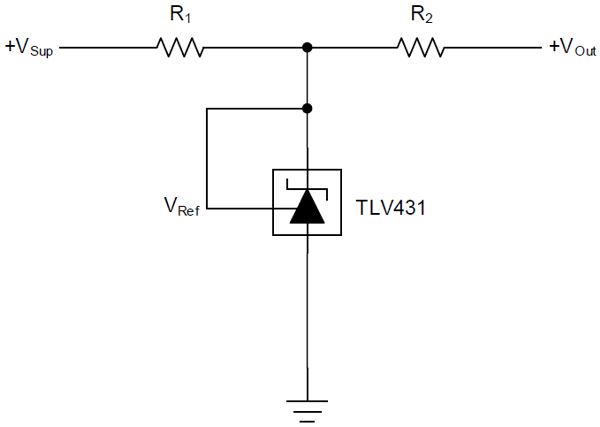
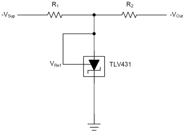
- Shunt regulators. One of the most cost-effective power-supply options is a shunt regulator. The cost savings come at the expense of the additional complexity required to design a reliable power-supply circuit. As an example, a precision ADC requiring bipolar supply operation might use the TLV431 – a low-voltage, adjustable shunt regulator – to generate ±2.5-V rails. You can use the TLV431 for this purpose because it has a low VREF. However, one challenge with this regulator is that it can supply only a limited amount of current. The TLV431 data sheet also requires a cathode current of ≥1 mA. These two restrictions limit the output-current capabilities of the standard setup shown in Figure 5 and Figure 6.
 Figure 5 Current-limited shunt
regulator circuit with positive output.
 Figure 6 Current-limited shunt
regulator circuit with negative output.
Figure 6 Current-limited shunt
regulator circuit with negative output.Figure 5 and Figure 6 show that both the cathode current and the current supplied to the ADC must flow through resistor R1. This configuration limits the supply current to (VSUP – VREF) / R1, resulting in two design challenges. First, current flowing continuously through R1 consumes power even with no applied load. Attempting to reduce R1 to increase the available supply current also proportionally increases the static power dissipation. Second, the maximum current set by R1 generally cannot support the hundreds of milliamperes of transient current that the ADC requires. An inability to provide the necessary current causes the supply voltage to droop, and can lead to unstable ADC operation.
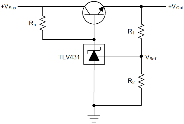
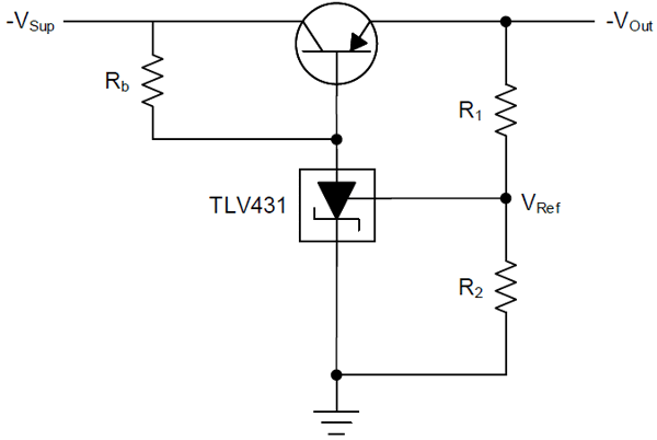
Mitigate these issues by adding two components to the circuit in Figure 5 and Figure 6. Figure 7 and Figure 8 show a modified shunt regulator circuit that includes a transistor and a bias resistor, Rb.
 Figure 7 Improved shunt regulator
circuit with positive output.
 Figure 8 Improved shunt regulator
circuit with negative output.
Figure 8 Improved shunt regulator
circuit with negative output.The power-supply circuit in Figure 7 and Figure 8 can provide more current compared to the system in Figure 5 and Figure 6 because the transistor eliminates any resistance between the supply input (VSUP) and output (VOUT). This new circuit can also maintain a cathode current of ≥1 mA by installing Rb instead of relying on R1. Resistors R1 and R2 therefore are only required to set the output voltage as per Equation 1.
For more information on how to use a voltage reference as a shunt regulator, see Related Website section below.