SNAU210B March 2020 – July 2021
- Trademarks
- 1Evaluation Board Setup
- 2EVM Description
- 3Bringing LMX2594 to a Lock State
- 4Loop Filter Configuration
- 5Key Results to Expect
- A Schematic
- B Bill of Materials
- C Board Layers Stack-Up
- D Changing Reference Oscillator and Setup
- E Connecting Reference Pro
- F Ramping Feature
- G SYSREF Feature
- H Enabling Onboard DC-DC Buck Converter (TPS62150)
- Revision History
4 Loop Filter Configuration
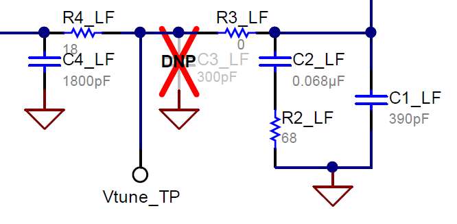
The parameters for the loop filters are:
Table 4-1 Loop Filter
Configuration
| PARAMETER | VALUE |
|---|---|
| VCO Gain | 132 MHz/V |
| Loop Bandwidth | 285 kHz |
| Phase Margin | 65 deg |
| C1_LF | 390 pF |
| C2_LF | 68 nF |
| C3_LF | Open |
| C4_LF | 1800 pF |
| R2 | 68 Ω |
| R3_LF | 0 Ω |
| R4_LF | 18 Ω |
| Effective Charge Pump Gain | 15 mA |
| Phase Detector Frequency (MHz) | 200 MHz |
| VCO Frequency | Designed for 15 GHz, but works over the whole frequency range |
 Figure 4-1 Loop
Filter Configuration
Figure 4-1 Loop
Filter ConfigurationFor detailed design and simulation of TI's PLLATINUM™ integrated circuits, see the PLLatinum Sim Tool.
For application notes, blogs, or videos on TI PLL products, see http://www.ti.com/pll.