SNLA266A January 2016 – December 2023 DP83822H , DP83822HF , DP83822I , DP83822IF , DP83825I , DP83826E , DP83826I
- 1
- DP8382x IEEE 802.3u Compliance and Debug
- Trademarks
- 1Terminology
- 2Standards and System Requirements
- 3Ethernet Physical Layer Compliance Testing
- 4How to Tune DP83825 VoD Swing
- 5IEEE802.3u Compliance Testing Scripts for the DP8382x
- 6References
- 7Revision History
3.2.3 Rise and Fall Time
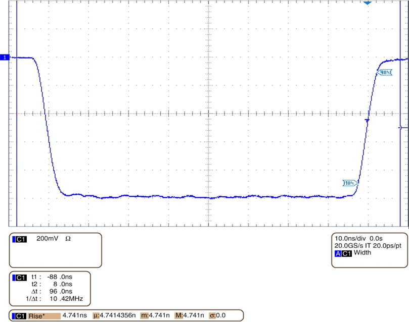
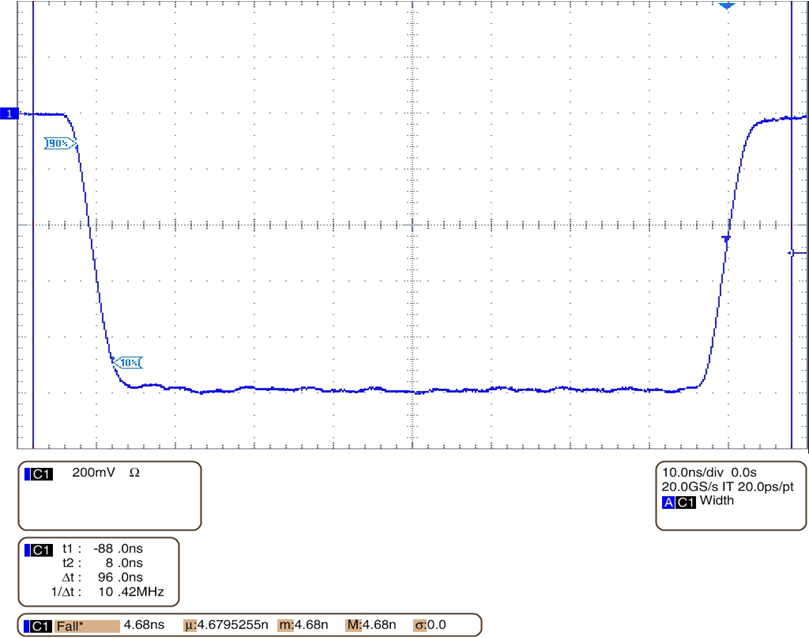
Purpose: To verify that the device rise and fall time are within the specified bounds.
Pass Condition: The rise and fall time (between 10% and 90% of the voltage levels for both positive and negative) must be between 3 ns and 5 ns. The maximum and minimum rise and fall times must be within 0.5 ns.
 Figure 3-4 100BASE-TX Rise Time Example Waveform
 Figure 3-5 100BASE-TX Fall Time Example Waveform