SNLA423 March 2023 DP83826E
- 1Trademarks
- 2DP83826 Application Overview
- 3Troubleshooting the Application
- 4Conclusion
- 5Revision History
3.7 Debugging MAC Interface
MII Link
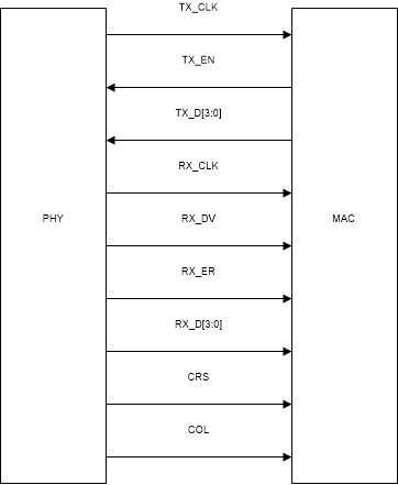
The Media Independent Interface (MII) is a synchronous 4-bit wide nibble data interface that connects the PHY to the MAC. The MII is fully compliant with IEEE 802.3-2002 clause 22.
MII is set by default in the PHY with Hardware Strap 8 RX_D2 = '0'. Register 0x0467, bit 8, can confirm the status of strap 8 (High or Low) and Register 0x0468, bit 4, can confirm the PHY's MAC Mode(MII = '0' | RMII = '1').
The MII signals are summarized below:
| FUNCTION | PINS |
|---|---|
| Data Signals | TX_D[3:0] |
| RX_D[3:0] | |
| Transmit and Receive Signals | TX_EN |
| RX_DV | |
| Line-Status Signals | CRS |
| COL | |
| Error Signals | RX_ER |
 Figure 3-7 MII Signaling
Reference the waveforms below to verify the expected MAC data and clock signals for 100BASE-Tx MII Mode. The table displays specs taken from the Datasheet that are shown in the waveforms.
| PARAMETER | TEST CONDITION | MIN | TYP | MAX | UNIT |
|---|---|---|---|---|---|
| T1 | RX_CLK High / Low Time | 16 | 20 | 24 | ns |
| T2 | RX_D[3:0], RX_ER, RX_DV Delay from RX_CLK rising | 10 | 30 | ns |
 Figure 3-8 RX_CLK High Time
 Figure 3-9 RX_D1 Delay from RX_CLK
rising
Figure 3-9 RX_D1 Delay from RX_CLK
risingRMII Link
Reduced Media Independent Interface, as specified in the RMII specification v1.2, provides a reduced pin count alternative to the IEEE 802.3 MII as specified in Clause 22. Architecturally, the RMII specification provides an additional reconciliation layer on either side of the MII, but can be implemented in the absence of an MII. The DP83826 offers two types of RMII operations: RMII Master and RMII Slave.
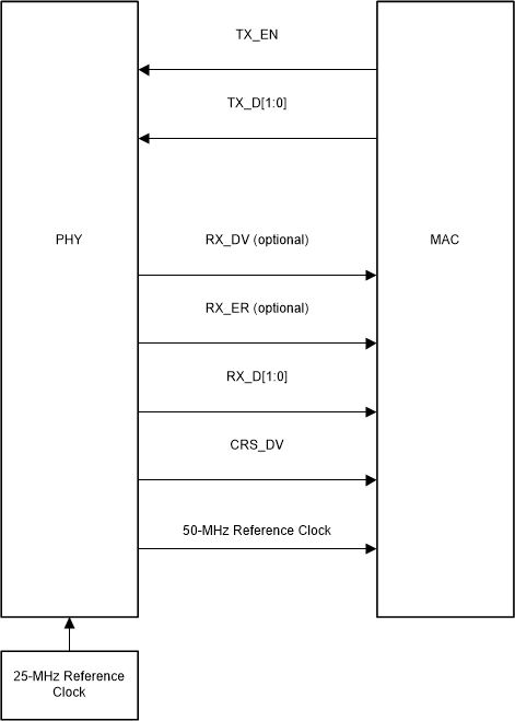
In RMII Master operation, the DP83826 operates from either a 25-MHz CMOS-level oscillator connected to XI pin or a 25-MHz crystal connected across XI and XO pins. A 50-MHz output clock referened from DP83826 can be connected to the MAC.
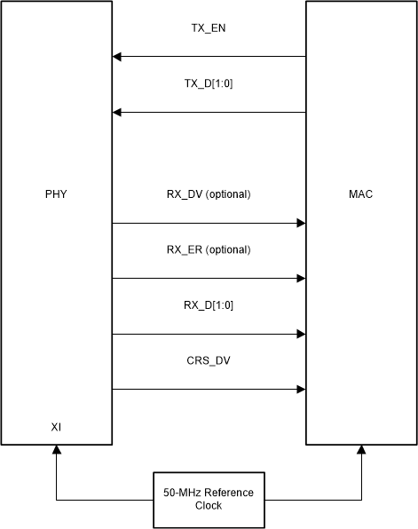
In RMII Slave operation, the DP83826 operates from a 50-MHz CMOS-level oscillator connected to the XI pin and shares the same clock as the MAC. Alternatively, the PHY can operate from a 50-MHz clock provided by the Host MAC.
The RMII specification has the following characteristics:
- Supports 100BASE-TX and 10BASE-Te
- Single clock reference sourced from the MAC to PHY (or from an external source)
- Provides independent 2-bit wide transmit and receive data paths
- Uses CMOS signal levels, the same levels as the MII interface
RMII can be set with pulling up Hardware Strap 8 RX_D2 = '1'. Register 0x0467, Bit 8 can confirm the Status of Strap 8 (High or Low) and Register 0x0468, can confirm the PHY's MAC Mode(MII = '0' | RMII = '1').
In this mode, data transfers are 2 bits for every clock cycle using the internal 50-MHz reference clock for both transmit and receive paths. The RMII signals are summarized below:
| FUNCTION | PINS |
|---|---|
| Receive data lines | TX_D[1:0] |
| Transmit data lines | RX_D[1:0] |
| Receive control signal | TX_EN |
| Transmit control signal | CRS_DV |
 Figure 3-10 RMII Slave Signaling
 Figure 3-11 RMII Master Signaling
Data on TX_D[1:0] are latched at the PHY with reference to the 50 MHz-clock in RMII master mode and slave mode. Data on RX_D[1:0] is provided in reference to 50-MHz clock. In addition, CRX_DV can be configured as RX_DV signal. It allows a simpler method of recovering receive data without the need to separate RX_DV from the CRS_DV indication.