SSZTB74 june 2016 LM22670 , LM22674 , LM22675 , LM22677 , LM22680 , LM25575 , LM25576 , LM2574 , LM2586 , LM2678 , LM2679 , LM2841 , LM2842 , LM2842-Q1 , LM43603 , LMR10510 , LMR12010 , LMR12020 , LMR14203 , LMR14206 , LMR62421 , LMV431
When designing a power supply, one of the challenges designers often face is dealing with voltage transients. It is important to protect circuitry from voltage spikes greater than the rated input voltage (VIN) of the integrated circuit (IC). When dealing with voltage transients, designers have a choice between using a DC/DC converter on the front end of the system with a wide-enough input voltage range to cover any transients, or a lower VIN DC/DC converter with additional clamping circuitry to provide transient protection.
At first glance, it may appear that choosing the first solution, a DC/DC converter with a wide VIN input rating of 36V or 60V, is more expensive because the 1ku price is higher than a converter with a lower voltage input rating. However, the extra voltage-clamp circuitry needed for the transient protection of a lower VIN converter can add 10 to 12 external components that will increase the bill-of-materials (BOM) count and cost, as well as solution size. In this post, I will compare the solution size and cost of the SIMPLE SWITCHER® LM43603 36 VIN, 3A buck converter against a comparable 17 VIN, 3A converter solution with additional clamping circuitry used to absorb the surge voltage.
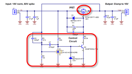
 Figure 1 Discrete Solution Used to
Clamp the Input Voltage
Figure 1 Discrete Solution Used to
Clamp the Input VoltageThe schematic in Figure 1 is an example of a discrete solution used to clamp the input voltage when the IC’s voltage rating is lower than the maximum input spike. This solution uses the LMV431 shunt regulator and a NPN transistor as a control circuit. The P-channel field-effect transistor (PFET) carries the pass-through current and has an increased voltage drop as the VIN surges and thus takes the increased power loss and protects the DC/DC converter. More detail on this technique can be found in the application note “Over Voltage Protection Circuit for Automotive Load Dump.”
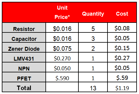
As seen in Figure 1, this input clamping control circuitry and PFET adds 13 extra external components to the solution. As Figure 2 shows, based on 1ku quantities published online, these 13 external components would add $1.19 to the total cost. The solution cost of a 17 VIN, 3A converter may be around $1.62, using 1ku-quantity pricing of $0.96 and including the cost of external components like the inductor, capacitors and resistors. This brings the total solution cost of using a 17 VIN buck converter plus clamping circuitry to approximately $1.62 + $1.19 = $2.81. Additionally, the control circuitry and PFET add approximately 210 mm2 to the solution size of the lower VIN solution. A 17 VIN, 3A converter may be around 100 mm2, which makes the total solution size 100 mm2+250 mm2 = 350 mm2.
 Figure 2 Control Circuit Cost
Breakdown
Figure 2 Control Circuit Cost
BreakdownAnother option is to use a DC/DC converter with a wider input-voltage range to cover the maximum VIN spike like the SIMPLE SWITCHER® LM43603 36 VIN, 3A synchronous buck converter. Using a wide-VIN device like the LM43603 enables designers to eliminate the additional clamping circuitry which saves time, cost and board space. The total solution cost of the LM43603 is approximately $2.51 using the published 1ku quantity price of $1.85 and including the cost of external components like the inductor, resistors and capacitors. This means that using the wider VIN LM43063 saves $0.30 or approximately 12%: $2.51 vs. $2.81. The benefits increase when you look at solution size. The total solution size of the LM43603 is approximately 250 mm2 which is about 24% or 60 mm2 smaller than the previous solution.
Another benefit to a wide VIN solution like the LM43603 is increased reliability. As I talked about in more detail in an earlier post, adding additional external components introduces additional risk into the system. The most reliable solution is the simplest solution with the fewest number of external components, because it reduces the risk of one component malfunctioning. Increasing reliability is very important particularly in the harsh conditions of some automotive and industrial applications. Plus, designing the additional clamping control circuitry adds significant work to the design cycle. Using the control circuitry and PFET means that you must select 12 more external components and run additional testing and simulations to ensure that it works. Why put in that effort when you can get a regulator with a wider VIN range with lower system costs and higher reliability?
Of course, pricing and solution size can vary widely based on volumes and contracts between vendors and suppliers, as well as design layouts. The size and cost percentage saved with a wide VIN solution will likewise vary. However, I hope this analysis shows that despite the higher upfront 1ku price, a wide VIN solution like the LM43603 can provide savings in solution cost, board space and design time when dealing with input-voltage transients.
Get more information on TI’s wide VIN DC/DC power solutions.