SLUS704C FEBRUARY 2007 – December 2014 UCC27423-EP , UCC27424-EP
PRODUCTION DATA.
- 1 Features
- 2 Applications
- 3 Description
- 4 Revision History
- 5 Pin Configuration and Functions
- 6 Specifications
- 7 Detailed Description
- 8 Application and Implementation
- 9 Power Supply Recommendations
- 10Layout
- 11Device and Documentation Support
- 12Mechanical, Packaging, and Orderable Information
Package Options
Mechanical Data (Package|Pins)
- D|8
Thermal pad, mechanical data (Package|Pins)
Orderable Information
1 Features
- Industry-Standard Pinout
- Enable Functions for Each Driver
- High Current-Drive Capability of ±4 A
- Unique Bipolar and CMOS True-Drive Output Stage Provides High Current at MOSFET Miller Thresholds
- TTL-/CMOS-Compatible Inputs Independent of Supply Voltage
- 20-ns Typical Rise and 15-ns Typical Fall Times With 1.8-nF Load
- Typical Propagation Delay Times of 25 ns With Input Falling and 35 ns With Input Rising
- 4.5-V to 15-V Supply Voltage
- Dual Outputs can be Paralleled for Higher Drive Current
- Available in Thermally-Enhanced MSOP PowerPAD™ Package With 4.7°C/W RθJC
- Supports Defense, Aerospace, and Medical Applications
- Controlled Baseline
- One Assembly/Test Site
- One Fabrication Site
- Extended Product Life Cycle
- Extended Product-Change Notification
- Product Traceability
2 Applications
- Switch-Mode Power Supplies
- DC/DC Converters
- Motor Controllers
- Line Drivers
- Class-D Switching Amplifiers
3 Description
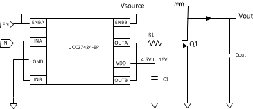
The UCC27423 and UCC27424 high-speed MOSFET drivers can deliver large peak currents into capacitive loads. Two standard logic options are offered – dual inverting and dual noninverting drivers. The UCC27424 thermally-enhanced 8-pin PowerPAD™ MSOP package (DGN) drastically lowers the thermal resistance to improve long-term reliability. The UCC27423 is offered in a standard SOIC-8 (D) package.
Using a design that inherently minimizes shoot-through current, this driver delivers 4 A of current where it is needed most – at the Miller plateau region during the MOSFET switching transition. A unique bipolar and MOSFET hybrid output stage in parallel also allows efficient current sourcing and sinking at low supply voltages.
The UCC27423 and UCC27424 provide enable (ENB) functions to better control the operation of the driver applications. ENBA and ENBB are implemented on pins 1 and 8, which previously were left unused in the industry-standard pinout. ENBA and ENBB are pulled up internally to VDD for active-high logic and can be left open for standard operation.
Device Information(1)
| PART NUMBER | PACKAGE | BODY SIZE (NOM) |
|---|---|---|
| UCC27423-EP | D (8) | 3.91 mm × 4.90 mm |
| UCC27424-EP | DGN (8) | 3.00 mm × 3.00 mm |
- For all available packages, see the orderable addendum at the end of the data sheet.
Simplified Schematic