SNAS825A December 2021 – April 2022 ADC128S102-SEP
PRODUCTION DATA
- 1 Features
- 2 Applications
- 3 Description
- 4 Revision History
- 5 Pin Configuration and Functions
- 6 Specifications
- 7 Detailed Description
- 8 Application and Implementation
- 9 Power Supply Recommendations
- 10Layout
- 11Device and Documentation Support
- 12Mechanical, Packaging, and Orderable Information
Package Options
Mechanical Data (Package|Pins)
- PW|16
Thermal pad, mechanical data (Package|Pins)
Orderable Information
3 Description
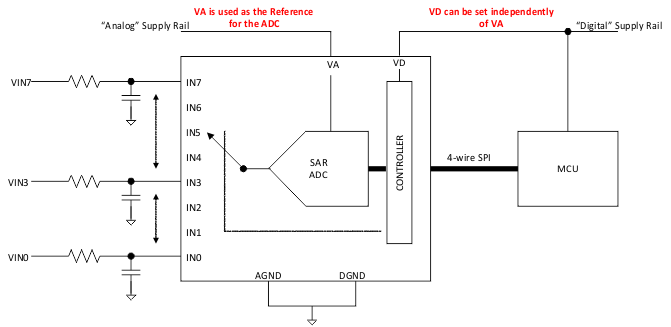
The ADC128S102-SEP is a low-power, eight-channel, CMOS, 12-bit analog-to-digital converter (ADC) specified for conversion throughput rates of 50 kSPS to 1 MSPS. The converter is based on a successive-approximation register (SAR) architecture with an internal track-and-hold circuit. The device can be configured to accept up to eight input signals at inputs IN0 through IN7.
The output serial data is straight binary and compatible with several standards, such as SPI, QSPI, MICROWIRE, and many common DSP serial interfaces.
The ADC128S102-SEP can be operated with independent analog and digital supplies. The analog supply (VA) can range from 2.7 V to 5.25 V, and the digital supply (VD) can range from 2.7 V to VA. Normal power consumption using a 3-V or 5-V supply is 2.3 mW and 10.7 mW, respectively. The power-down feature reduces the power consumption to 16.5 μW using a 3-V supply and 30 μW using a 5-V supply.
| PART NUMBER | PACKAGE | BODY SIZE (NOM) |
|---|---|---|
| ADC128S102-SEP | TSSOP (16) | 5.00 mm × 4.40 mm |
 Block Diagram