SBAS683B August   2014  – May 2020 ADS1120-Q1

PRODUCTION DATA.  

  1. Features
  2. Applications
  3. Description
    1.     Device Images
      1.      Block Diagram
  4. Revision History
  5. Pin Configuration and Functions
    1.     Pin Functions
  6. Specifications
    1. 6.1 Absolute Maximum Ratings
    2. 6.2 ESD Ratings
    3. 6.3 Recommended Operating Conditions
    4. 6.4 Thermal Information
    5. 6.5 Electrical Characteristics
    6. 6.6 SPI Timing Requirements
    7. 6.7 SPI Switching Characteristics
    8. 6.8 Typical Characteristics
  7. Parameter Measurement Information
    1. 7.1 Noise Performance
  8. Detailed Description
    1. 8.1 Overview
    2. 8.2 Functional Block Diagram
    3. 8.3 Feature Description
      1. 8.3.1  Multiplexer
      2. 8.3.2  Low-Noise PGA
        1. 8.3.2.1 PGA Common-Mode Voltage Requirements
        2. 8.3.2.2 Bypassing the PGA
      3. 8.3.3  Modulator
      4. 8.3.4  Digital Filter
      5. 8.3.5  Output Data Rate
      6. 8.3.6  Voltage Reference
      7. 8.3.7  Clock Source
      8. 8.3.8  Excitation Current Sources
      9. 8.3.9  Low-Side Power Switch
      10. 8.3.10 Sensor Detection
      11. 8.3.11 System Monitor
      12. 8.3.12 Offset Calibration
      13. 8.3.13 Power Supplies
      14. 8.3.14 Temperature Sensor
        1. 8.3.14.1 Converting from Temperature to Digital Codes
          1. 8.3.14.1.1 For Positive Temperatures (for Example, 50°C):
          2. 8.3.14.1.2 For Negative Temperatures (for Example, –25°C):
        2. 8.3.14.2 Converting from Digital Codes to Temperature
    4. 8.4 Device Functional Modes
      1. 8.4.1 Power-Up and Reset
      2. 8.4.2 Conversion Modes
        1. 8.4.2.1 Single-Shot Mode
        2. 8.4.2.2 Continuous-Conversion Mode
      3. 8.4.3 Operating Modes
        1. 8.4.3.1 Normal Mode
        2. 8.4.3.2 Duty-Cycle Mode
        3. 8.4.3.3 Turbo Mode
        4. 8.4.3.4 Power-Down Mode
    5. 8.5 Programming
      1. 8.5.1 Serial Interface
        1. 8.5.1.1 Chip Select (CS)
        2. 8.5.1.2 Serial Clock (SCLK)
        3. 8.5.1.3 Data Ready (DRDY)
        4. 8.5.1.4 Data Input (DIN)
        5. 8.5.1.5 Data Output and Data Ready (DOUT/DRDY)
        6. 8.5.1.6 SPI Timeout
      2. 8.5.2 Data Format
      3. 8.5.3 Commands
        1. 8.5.3.1 RESET (0000 011x)
        2. 8.5.3.2 START/SYNC (0000 100x)
        3. 8.5.3.3 POWERDOWN (0000 001x)
        4. 8.5.3.4 RDATA (0001 xxxx)
        5. 8.5.3.5 RREG (0010 rrnn)
        6. 8.5.3.6 WREG (0100 rrnn)
      4. 8.5.4 Reading Data
      5. 8.5.5 Sending Commands
      6. 8.5.6 Interfacing with Multiple Devices
    6. 8.6 Register Map
      1. 8.6.1 Configuration Registers
        1. 8.6.1.1 Configuration Register 0 (Address = 00h) [reset = 00h]
          1. Table 12. Configuration Register 0 Field Descriptions
        2. 8.6.1.2 Configuration Register 1 (Address = 01h) [reset = 00h]
          1. Table 13. Configuration Register 1 Field Descriptions
        3. 8.6.1.3 Configuration Register 2 (Address = 02h) [reset = 00h]
          1. Table 15. Configuration Register 2 Field Descriptions
        4. 8.6.1.4 Configuration Register 3 (Address = 03h) [reset = 00h]
          1. Table 16. Configuration Register 3 Field Descriptions
  9. Application and Implementation
    1. 9.1 Application Information
      1. 9.1.1 Serial Interface Connections
      2. 9.1.2 Analog Input Filtering
      3. 9.1.3 External Reference and Ratiometric Measurements
      4. 9.1.4 Establishing a Proper Common-Mode Input Voltage
      5. 9.1.5 Unused Inputs and Outputs
      6. 9.1.6 Pseudo Code Example
    2. 9.2 Typical Applications
      1. 9.2.1 K-Type Thermocouple Measurement (–200°C to +1250°C)
        1. 9.2.1.1 Design Requirements
        2. 9.2.1.2 Detailed Design Procedure
        3. 9.2.1.3 Application Curves
      2. 9.2.2 3-Wire RTD Measurement (–200°C to +850°C)
        1. 9.2.2.1 Design Requirements
        2. 9.2.2.2 Detailed Design Procedure
          1. 9.2.2.2.1 Design Variations for 2-Wire and 4-Wire RTD Measurements
        3. 9.2.2.3 Application Curves
      3. 9.2.3 Bridge Measurement
        1. 9.2.3.1 Design Requirements
        2. 9.2.3.2 Detailed Design Procedure
  10. 10Power Supply Recommendations
    1. 10.1 Power-Supply Sequencing
    2. 10.2 Power-Supply Ramp Rate
    3. 10.3 Power-Supply Decoupling
  11. 11Layout
    1. 11.1 Layout Guidelines
    2. 11.2 Layout Example
  12. 12Device and Documentation Support
    1. 12.1 Documentation Support
      1. 12.1.1 Related Documentation
    2. 12.2 Receiving Notification of Documentation Updates
    3. 12.3 Support Resources
    4. 12.4 Trademarks
    5. 12.5 Electrostatic Discharge Caution
    6. 12.6 Glossary
  13. 13Mechanical, Packaging, and Orderable Information

Package Options

Mechanical Data (Package|Pins)
Thermal pad, mechanical data (Package|Pins)
Orderable Information

Design Variations for 2-Wire and 4-Wire RTD Measurements

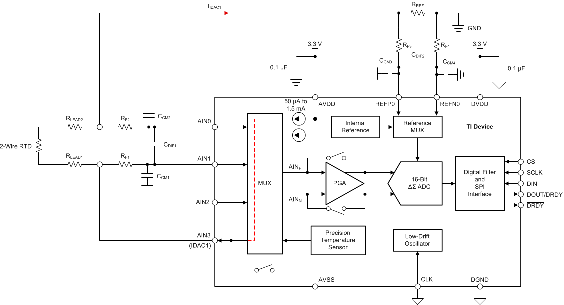
Implementing a 2- or 4-wire RTD measurement is very similar to the 3-wire RTD measurement illustrated in Figure 77, except that only one IDAC is required.

Figure 78 shows a typical circuit implementation of a 2-wire RTD measurement. The main difference compared to a 3-wire RTD measurement is with respect to the lead resistance compensation. The voltage drop across the lead resistors, RLEAD1 and RLEAD2, in this configuration is directly part of the measurement (as shown in Equation 40) because there is no means to compensate the lead resistance by use of the second current source. Any compensation must be done by calibration.

Equation 40. VIN = IIDAC1 · (RLEAD1 + RRTD + RLEAD2)
ADS1120-Q1 ai_2W_RTD_example_bas535.gifFigure 78. 2-Wire RTD Measurement

Figure 79 illustrates a typical circuit implementation of a 4-wire RTD measurement. Similar to the 2-wire RTD measurement, only one IDAC is required for exciting and measuring a 4-wire RTD in a ratiometric manner. The main benefit of using a 4-wire RTD is that the ADC inputs are connected to the RTD in the form of a Kelvin connection. Apart from the input leakage currents of the ADC, there is no current flow through the lead resistors RLEAD2 and RLEAD3 and therefore no voltage drop is created across them. The voltage at the ADC inputs consequently equals the voltage across the RTD and the lead resistance is of no concern.

Note that because only one IDAC is used and flows through the reference resistor, RREF, the transfer function of a 2- and 4-wire RTD measurement differs compared to the one of a 3-wire RTD measurement by a factor of 2, as shown in Equation 41.

Equation 41. Code ∝ (RRTD (at Temperature) · Gain) / RREF

In addition, the common-mode and reference voltage is reduced compared to the 3-wire RTD configuration. Therefore, some further modifications may be required in case the 3-wire RTD design is used to measure 2- and 4-wire RTDs as well. If the decreased common-mode voltage does not meet the VCM (MIN) requirements of the PGA anymore, either increase the value of RREF by switching in a larger resistor or, alternatively, increase the excitation current while decreasing the gain at the same time.
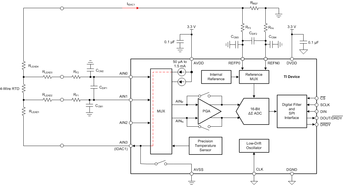
ADS1120-Q1 ai_4W_RTD_example_bas535.gifFigure 79. 4-Wire RTD Measurement