SBAS350G June 2005 – January 2021 ADS1232 , ADS1234
PRODUCTION DATA
- 1 Features
- 2 Applications
- 3 Description
- 4 Revision History
- 5 Pin Configuration and Functions
- 6 Specifications
- 7 Parameter Measurement Information
-
8 Detailed Description
- 8.1 Overview
- 8.2 Functional Block Diagram
- 8.3
Feature Description
- 8.3.1 Analog Inputs (AINPX, AINNX)
- 8.3.2 Temperature Sensor (ADS1232 Only)
- 8.3.3 Low-Noise PGA
- 8.3.4 Voltage Reference Inputs (REFP, REFN)
- 8.3.5 Clock Sources
- 8.3.6 Digital Filter Frequency Response
- 8.3.7 Settling Time
- 8.3.8 Data Rate
- 8.3.9 Data Format
- 8.3.10 Data Ready and Data Output (DRDY/DOUT)
- 8.3.11 Serial Clock Input (SCLK)
- 8.3.12 Data Retrieval
- 8.4 Device Functional Modes
- 9 Application and Implementation
- 10Power Supply Recommendations
- 11Layout
- 12Device and Documentation Support
- 13Mechanical, Packaging, and Orderable Information
Package Options
Mechanical Data (Package|Pins)
- PW|24
Thermal pad, mechanical data (Package|Pins)
- PW|24
Orderable Information
8.3.6 Digital Filter Frequency Response
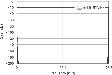
The ADS123x use a sinc4 digital filter with the frequency response (fCLK = 4.9152 MHz) shown in Figure 8-5. The frequency response repeats at multiples of the modulator sampling frequency of 76.8 kHz. The overall response is that of a low-pass filter with a –3-dB cutoff frequency of 2.4 Hz with the SPEED pin tied low (10-SPS data rate) and 19 Hz with the SPEED pin tied high (80-SPS data rate).
 Figure 8-5 Digital Filter Frequency Response
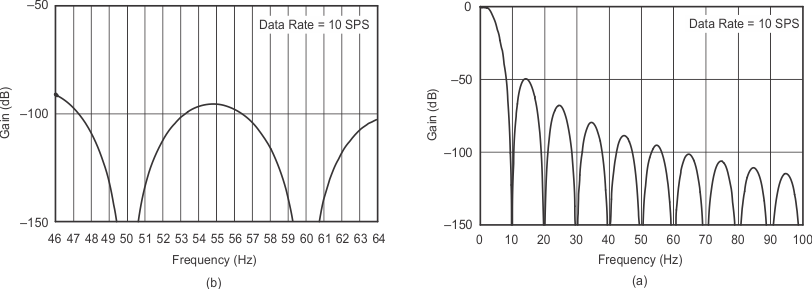
To better demonstrate the response at lower frequencies, Figure 8-6(a) illustrates the response out to 100 Hz, when the data rate = 10 SPS. Notice that signals at multiples of 10 Hz are rejected, and therefore, simultaneous rejection of 50 Hz and 60 Hz interference is achieved.
The benefit of using a sinc4 filter is that every frequency notch has four zeros at the same location. This response, combined with the low-drift internal oscillator, provides an excellent normal-mode rejection of line-cycle interference.
Figure 8-6(b) shows the plot enlarged for both 50-Hz and 60-Hz notches with the SPEED pin tied low (10-SPS data rate). With only a ±3% variation of the internal oscillator, over 100 dB of normal-mode rejection is achieved.
 Figure 8-6 Digital
Filter Frequency Response to 100 Hz
Figure 8-6 Digital
Filter Frequency Response to 100 HzThe ADS123x data rate and frequency response scale directly with clock frequency. For example, if fCLK increases from 4.9152 MHz to 6.144 MHz when the SPEED pin is tied high, the data rate increases from 80 SPS to 100 SPS, while filter notches also increase from 80 Hz to 100 Hz. Frequency scaling is only possible when the external clock source is applied.