SBAS778B June   2017  – August 2019 ADS1287

PRODUCTION DATA.  

  1. Features
  2. Applications
  3. Description
    1.     Device Images
      1.      Functional Block Diagram
  4. Revision History
  5. Pin Configuration and Functions
    1.     Pin Functions
  6. Specifications
    1. 6.1 Absolute Maximum Ratings
    2. 6.2 ESD Ratings
    3. 6.3 Recommended Operating Conditions
    4. 6.4 Thermal Information
    5. 6.5 Electrical Characteristics
    6. 6.6 Timing Requirements
    7. 6.7 Switching Characteristics
    8. 6.8 Typical Characteristics
  7. Parameter Measurement Information
    1. 7.1 Noise Performance
  8. Detailed Description
    1. 8.1 Overview
    2. 8.2 Functional Block Diagram
    3. 8.3 Feature Description
      1. 8.3.1 Analog Input and Multiplexer
      2. 8.3.2 Programmable Gain Amplifier (PGA)
      3. 8.3.3 Modulator
        1. 8.3.3.1 Modulator Overrange
      4. 8.3.4 Voltage Reference Inputs (REFP, REFN)
      5. 8.3.5 Digital Filter
        1. 8.3.5.1 Sinc Filter Stage
        2. 8.3.5.2 FIR Filter Stage
        3. 8.3.5.3 Group Delay and Step Response
          1. 8.3.5.3.1 Linear Phase Response
          2. 8.3.5.3.2 Minimum Phase Response
        4. 8.3.5.4 HPF Stage
      6. 8.3.6 Reset (RESET Pin and Reset Command)
      7. 8.3.7 Master Clock Input (CLK)
    4. 8.4 Device Functional Modes
      1. 8.4.1  Operational Mode
      2. 8.4.2  Chop Mode
      3. 8.4.3  Offset
      4. 8.4.4  Power-Down Mode
      5. 8.4.5  Standby Mode
      6. 8.4.6  Synchronization
        1. 8.4.6.1 Pulse-Sync Mode
        2. 8.4.6.2 Continuous-Sync Mode
      7. 8.4.7  Reading Data
        1. 8.4.7.1 Read-Data-Continuous Mode (RDATAC)
        2. 8.4.7.2 Stop-Read-Data-Continuous-Mode (SDATAC)
      8. 8.4.8  Conversion Data Format
      9. 8.4.9  Offset and Full-Scale Calibration Registers
        1. 8.4.9.1 OFC[2:0] Registers
        2. 8.4.9.2 FSC[2:0] Registers
      10. 8.4.10 Calibration Command
        1. 8.4.10.1 OFSCAL Command
        2. 8.4.10.2 GANCAL Command
      11. 8.4.11 User Calibration
    5. 8.5 Programming
      1. 8.5.1 Serial Interface
        1. 8.5.1.1 Chip Select (CS)
        2. 8.5.1.2 Serial Clock (SCLK)
        3. 8.5.1.3 Data Input (DIN)
        4. 8.5.1.4 Data Output (DOUT)
        5. 8.5.1.5 Serial Interface Timeout
        6. 8.5.1.6 Data Ready (DRDY)
      2. 8.5.2 Commands
        1. 8.5.2.1  WAKEUP: Wake Up Command
        2. 8.5.2.2  STANDBY: Standby Mode Command
        3. 8.5.2.3  SYNC: Synchronize ADC Conversions
        4. 8.5.2.4  RESET: Reset Command
        5. 8.5.2.5  RDATAC: Read Data Continuous Mode Command
        6. 8.5.2.6  SDATAC: Stop Read Data Continuous Mode Command
        7. 8.5.2.7  RDATA: Read Data Command
        8. 8.5.2.8  RREG: Read Register Data Command
        9. 8.5.2.9  WREG: Write Register Data Command
        10. 8.5.2.10 OFSCAL: Offset Calibration Command
        11. 8.5.2.11 GANCAL: Gain Calibration Command
    6. 8.6 Register Map
      1. 8.6.1 Register Descriptions
        1. 8.6.1.1 ID/CFG: ID, Configuration Register (address = 00h) [reset = x0h]
          1. Table 22. ID/CFG Register Field Descriptions
        2. 8.6.1.2 CONFIG0: Configuration Register 0 (address = 01h) [reset = 52h]
          1. Table 23. CONFIG0 Register Field Descriptions
        3. 8.6.1.3 CONFIG1: Configuration Register 1 (address = 02h) [reset = 08h]
          1. Table 24. CONFIG1 Register Field Descriptions
        4. 8.6.1.4 High-Pass Filter Corner Frequency (HPFx) Registers (address = 03h, 04h) [reset = 32h, 03h]
          1. Table 25. HPF0, HPF1 Registers Field Description
        5. 8.6.1.5 Offset Calibration (OFCx) Registers (address = 05h, 06h, 07h) [reset = 00h, 00h, 00h]
          1. Table 26. OFC0, OFC1, OFC2 Registers Field Description
        6. 8.6.1.6 Full-Scale Calibration (FSCx) Registers (address = 08h, 09h, 0Ah) [reset = 00h, 00h, 40h]
          1. Table 27. FSC0, FSC1, FSC2 Registers Field Description
  9. Application and Implementation
    1. 9.1 Application Information
    2. 9.2 Typical Applications
      1. 9.2.1 Geophone Application
      2. 9.2.2 Digital Interface
    3. 9.3 Initialization Set Up
  10. 10Power Supply Recommendations
    1. 10.1 Analog Power Supplies
    2. 10.2 Digital Power Supply
    3. 10.3 Power-Supply Sequence
  11. 11Layout
    1. 11.1 Layout Guidelines
  12. 12Device and Documentation Support
    1. 12.1 Receiving Notification of Documentation Updates
    2. 12.2 Community Resources
    3. 12.3 Trademarks
    4. 12.4 Electrostatic Discharge Caution
    5. 12.5 Glossary
  13. 13Mechanical, Packaging, and Orderable Information

Package Options

Mechanical Data (Package|Pins)
Thermal pad, mechanical data (Package|Pins)
Orderable Information

Data Ready (DRDY)

DRDY is an output that indicates when new conversion data are ready. DRDY is always actively driven regardless whether CS is high or low. When reading data in the read data continuous mode, the read operation must be completed four CLK periods prior to the next DRDY falling edge, or the data are overwritten by new conversion data.

During data readback, DRDY is driven high on the first falling edge of SCLK. Figure 63 and Figure 64 show the function of DRDY with and without data readback, respectively. If data are not retrieved (no SCLK provided), as shown in Figure 64, DRDY pulses high for four fCLK periods during the update time.
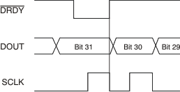
ADS1287 ai_tim_drdy_bas418.gifFigure 63. DRDY With Data Retrieval
ADS1287 ai_tim_drdy_nortrv_bas418.gifFigure 64. DRDY With No Data Retrieval