SBAS705B June   2015  – April 2020 ADS131E08S

PRODUCTION DATA.  

  1. Features
  2. Applications
    1.     Power Application: Three-Phase Voltage and Current Connection
  3. Description
  4. Revision History
  5. Device Comparison
  6. Pin Configuration and Functions
    1.     Pin Functions
  7. Specifications
    1. 7.1 Absolute Maximum Ratings
    2. 7.2 ESD Ratings
    3. 7.3 Recommended Operating Conditions
    4. 7.4 Thermal Information
    5. 7.5 Electrical Characteristics
    6. 7.6 Timing Requirements
    7. 7.7 Switching Characteristics
    8. 7.8 Typical Characteristics
  8. Parameter Measurement Information
    1. 8.1 Noise Measurements
  9. Detailed Description
    1. 9.1 Overview
    2. 9.2 Functional Block Diagram
    3. 9.3 Feature Description
      1. 9.3.1  Electromagnetic Interference (EMI) Filter
      2. 9.3.2  Input Multiplexer
        1. 9.3.2.1 Device Noise Measurements
        2. 9.3.2.2 Test Signals (TestP and TestN)
        3. 9.3.2.3 Temperature Sensor (TempP, TempN)
        4. 9.3.2.4 Power-Supply Measurements (MVDDP, MVDDN)
      3. 9.3.3  Analog Input
      4. 9.3.4  PGA Settings and Input Range
        1. 9.3.4.1 Input Common-Mode Range
      5. 9.3.5  ΔΣ Modulator
      6. 9.3.6  Clock
      7. 9.3.7  Digital Decimation Filter
      8. 9.3.8  Voltage Reference
      9. 9.3.9  Input Out-of-Range Detection
      10. 9.3.10 General-Purpose Digital I/O (GPIO)
    4. 9.4 Device Functional Modes
      1. 9.4.1 Power-Down
      2. 9.4.2 Reset
      3. 9.4.3 Conversion Mode
        1. 9.4.3.1 START Pin Low-to-High Transition or START Command Sent
        2. 9.4.3.2 Input Signal Step
        3. 9.4.3.3 Continuous Conversion Mode
    5. 9.5 Programming
      1. 9.5.1 SPI Interface
        1. 9.5.1.1 Chip Select (CS)
        2. 9.5.1.2 Serial Clock (SCLK)
        3. 9.5.1.3 Data Input (DIN)
        4. 9.5.1.4 Data Output (DOUT)
        5. 9.5.1.5 Data Ready (DRDY)
      2. 9.5.2 Data Retrieval
        1. 9.5.2.1 Status Word
        2. 9.5.2.2 Readback Length
        3. 9.5.2.3 Data Format
      3. 9.5.3 SPI Command Definitions
        1. 9.5.3.1  WAKEUP: Exit STANDBY Mode
        2. 9.5.3.2  STANDBY: Enter STANDBY Mode
        3. 9.5.3.3  RESET: Reset Registers to Default Values
        4. 9.5.3.4  START: Start Conversions
        5. 9.5.3.5  STOP: Stop Conversions
        6. 9.5.3.6  OFFSETCAL: Channel Offset Calibration
        7. 9.5.3.7  RDATAC: Start Read Data Continuous Mode
        8. 9.5.3.8  SDATAC: Stop Read Data Continuous Mode
        9. 9.5.3.9  RDATA: Read Data
        10. 9.5.3.10 RREG: Read from Register
        11. 9.5.3.11 WREG: Write to Register
        12. 9.5.3.12 Sending Multibyte Commands
    6. 9.6 Register Map
      1. 9.6.1 Register Descriptions
        1. 9.6.1.1 ID: ID Control Register (Factory-Programmed, Read-Only) (address = 00h) [reset = D2h]
          1. Table 11. ID: ID Control Register Field Descriptions
        2. 9.6.1.2 CONFIG1: Configuration Register 1 (address = 01h) [reset = 94h]
          1. Table 12. CONFIG1: Configuration Register 1 Field Descriptions
        3. 9.6.1.3 CONFIG2: Configuration Register 2 (address = 02h) [reset = 00h]
          1. Table 14. CONFIG2: Configuration Register 2 Field Descriptions
        4. 9.6.1.4 CONFIG3: Configuration Register 3 (address = 03h) [reset = E0h]
          1. Table 15. CONFIG3: Configuration Register 3 Field Descriptions
        5. 9.6.1.5 FAULT: Fault Detect Control Register (address = 04h) [reset = 00h]
          1. Table 16. FAULT: Fault Detect Control Register Field Descriptions
        6. 9.6.1.6 CHnSET: Individual Channel Settings (address = 05h to 0Ch) [reset = 10h]
          1. Table 17. CHnSET: Individual Channel Settings Field Descriptions
        7. 9.6.1.7 FAULT_STATP: Fault Detect Positive Input Status (address = 12h) [reset = 00h]
          1. Table 18. FAULT_STATP: Fault Detect Positive Input Status Field Descriptions
        8. 9.6.1.8 FAULT_STATN: Fault Detect Negative Input Status (address = 13h) [reset = 00h]
          1. Table 19. FAULT_STATN: Fault Detect Negative Input Status Field Descriptions
        9. 9.6.1.9 GPIO: General-Purpose IO Register (address = 14h) [reset = 0Fh]
          1. Table 20. GPIO: General-Purpose IO Register Field Descriptions
  10. 10Application and Implementation
    1. 10.1 Application Information
      1. 10.1.1 Multiple Device Configuration
        1. 10.1.1.1 Synchronizing Multiple Devices
        2. 10.1.1.2 Standard Configuration
        3. 10.1.1.3 Daisy-Chain Configuration
      2. 10.1.2 Power Monitoring Specific Applications
      3. 10.1.3 Current Sensing
      4. 10.1.4 Voltage Sensing
    2. 10.2 Typical Application
      1. 10.2.1 Design Requirements
      2. 10.2.2 Detailed Design Procedure
      3. 10.2.3 Application Curves
    3. 10.3 Initialization Set Up
      1. 10.3.1 Setting the Device Up for Basic Data Capture
  11. 11Power Supply Recommendations
    1. 11.1 Power-Up Timing
    2. 11.2 Recommended External Capacitor Values
    3. 11.3 Device Connections for Unipolar Power Supplies
    4. 11.4 Device Connections for Bipolar Power Supplies
  12. 12Layout
    1. 12.1 Layout Guidelines
    2. 12.2 Layout Example
  13. 13Device and Documentation Support
    1. 13.1 Documentation Support
      1. 13.1.1 Related Documentation
    2. 13.2 Support Resources
    3. 13.3 Trademarks
    4. 13.4 Electrostatic Discharge Caution
    5. 13.5 Glossary
  14. 14Mechanical, Packaging, and Orderable Information

Package Options

Mechanical Data (Package|Pins)
Thermal pad, mechanical data (Package|Pins)
Orderable Information

Continuous Conversion Mode

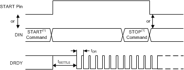
When the START pin is pulled high or the START command is issued, conversions continue indefinitely until the START pin is taken low or the STOP command is transmitted, as shown in Figure 34. When the START pin is pulled low or the STOP command is issued, the conversion in progress completes and the DRDY output transitions from high to low indicating that the latest data are available. Figure 35 and Table 6 illustrate the timing of where the START pin can be brought low or the STOP command can be sent relative to a completed conversion to halt further conversions. If the START pin is pulled low or if the STOP command is sent after the tDSHD time, then an additional conversion takes place and completes before further conversions are halted. To continuously run the converter without commands, tie the START pin high.
ADS131E08S ai_tim_cont_conv_sbas705.gif
START and STOP commands take effect on the seventh SCLK falling edge.
Figure 34. Continuous Conversion Mode
ADS131E08S ai_tim_start-drdy_bas561.gif
START and STOP commands take effect on the seventh SCLK falling edge at the end of the transmission.
Figure 35. START to DRDY Timing

Table 6. Timing Characteristics for Figure 35(1)

MIN UNIT
tSDSU Setup time; set the START pin low or send the STOP command before the DRDY falling edge to halt further conversions 16 tCLK
tDSHD Delay time; set the START pin low or send the STOP command to complete the current conversion and halt further conversions 16 tCLK
START and STOP commands take effect on the seventh SCLK falling edge at the end of the transmission.