SBAS486F November 2009 – February 2016 ADS41B29 , ADS41B49
PRODUCTION DATA.
- 1 Features
- 2 Applications
- 3 Description
- 4 Revision History
- 5 Pin Configuration and Functions
-
6 Specifications
- 6.1 Absolute Maximum Ratings
- 6.2 ESD Ratings
- 6.3 Recommended Operating Conditions
- 6.4 Thermal Information
- 6.5 Electrical Characteristics: General
- 6.6 Electrical Characteristics: ADS41B29, ADS41B49
- 6.7 Digital Characteristics
- 6.8 Timing Requirements: LVDS and CMOS Modes
- 6.9 Timing Requirements: Reset
- 6.10 Timing Requirements: LVDS Timing Across Sampling Frequencies
- 6.11 Timing Requirements: CMOS Timing Across Sampling Frequencies
- 6.12 Timing Requirements: CMOS Timing Across Sampling Frequencies
- 6.13 Typical Characteristics: ADS41B49
- 6.14 Typical Characteristics: ADS41B29
- 6.15 Typical Characteristics: General
- 6.16 Typical Characteristics: Contour
- 7 Parameter Measurement Information
-
8 Detailed Description
- 8.1 Overview
- 8.2 Functional Block Diagram
- 8.3 Feature Description
- 8.4 Device Functional Modes
- 8.5 Programming
- 8.6
Register Maps
- 8.6.1
Serial Register Map
- 8.6.1.1 Summary of High-Performance Modes
- 8.6.1.2
Description of Serial Registers
- 8.6.1.2.1 Register Address 00h (address = 00h) [reset = 00h]
- 8.6.1.2.2 Register Address 01h (address = 01h) [reset = 00h]
- 8.6.1.2.3 Register Address 03h (address = 03h) [reset = 00h]
- 8.6.1.2.4 Register Address 25h (address = 25h) [reset = 50h]
- 8.6.1.2.5 Register Address 26h (address = 26h) [reset = 00h]
- 8.6.1.2.6 Register Address 3Dh (address = 3Dh) [reset = 00h]
- 8.6.1.2.7 Register Address 3Fh (address = 3Fh) [reset = 00h]
- 8.6.1.2.8 Register Address 40h (address = 40h) [reset = 00h]
- 8.6.1.2.9 Register Address 41h (address = 41h) [reset = 00h]
- 8.6.1.2.10 Register Address 42h (address = 42h) [reset = 08h]
- 8.6.1.2.11 Register Address 43h (address = 43h) [reset = 00h]
- 8.6.1.2.12 Register Address 4Ah (address = 4Ah) [reset = 00h]
- 8.6.1.2.13 Register Address BFh (address = BFh) [reset = 00h]
- 8.6.1.2.14 Register Address CFh (address = CFh) [reset = 00h]
- 8.6.1.2.15 Register Address DFh (address = DFh) [reset = 00h]
- 8.6.1
Serial Register Map
- 9 Application and Implementation
- 10Power Supply Recommendations
- 11Layout
- 12Device and Documentation Support
- 13Mechanical, Packaging, and Orderable Information
Package Options
Mechanical Data (Package|Pins)
- RGZ|48
Thermal pad, mechanical data (Package|Pins)
- RGZ|48
Orderable Information
5 Pin Configuration and Functions
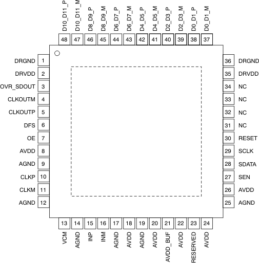
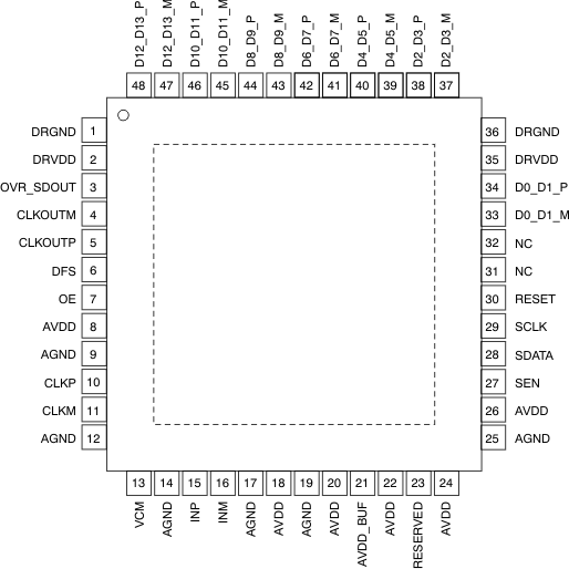
ADS41B29 LVDS Mode: RGZ Package(2)1
48-Pin VQFN
Top View

1.
NOINDENT:
The PowerPAD is connected to DRGND.Pin Functions
| PIN | NO. | I/O | DESCRIPTION | |
|---|---|---|---|---|
| NAME | ADS41B49 | ADS41B29 | ||
| AGND | 9, 12, 14, 17, 19, 25 | 9, 12, 14, 17, 19, 25 | I | Analog ground |
| AVDD | 8, 18, 20, 22, 24, 26 | 8, 18, 20, 22, 24, 26 | I | 1.8-V analog power supply |
| AVDD_BUF | 21 | 21 | I | 3.3-V input buffer supply |
| CLKM | 11 | 11 | I | Differential clock input, negative |
| CLKP | 10 | 10 | I | Differential clock input, positive |
| CLKOUTP | 5 | 5 | O | Differential output clock, true |
| CLKOUTM | 4 | 4 | O | Differential output clock, complement |
| D0_D1_M | 33 | 37 | O | Differential output data D0 and D1 multiplexed, complement |
| D0_D1_P | 34 | 38 | O | Differential output data D0 and D1 multiplexed, true |
| D2_D3_M | 37 | 39 | O | Differential output data D2 and D3 multiplexed, complement |
| D2_D3_P | 38 | 40 | O | Differential output data D2 and D3 multiplexed, true |
| D4_D5_M | 39 | 41 | O | Differential output data D4 and D5 multiplexed, complement |
| D4_D5_P | 40 | 42 | O | Differential output data D4 and D5 multiplexed, true |
| D6_D7_M | 41 | 43 | O | Differential output data D6 and D7 multiplexed, complement |
| D6_D7_P | 42 | 44 | O | Differential output data D6 and D7 multiplexed, true |
| D8_D9_M | 43 | 45 | O | Differential output data D8 and D9 multiplexed, complement |
| D8_D9_P | 44 | 46 | O | Differential output data D8 and D9 multiplexed, true |
| D10_D11_M | 45 | 47 | O | Differential output data D10 and D11 multiplexed, complement |
| D10_D11_P | 46 | 48 | O | Differential output data D10 and D11 multiplexed, true |
| D12_D13_M | 47 | — | O | Differential output data D12 and D13 multiplexed, complement |
| D12_D13_P | 48 | — | O | Differential output data D12 and D13 multiplexed, true |
| DFS | 6 | 6 | I | Data format select input. This pin sets the DATA FORMAT (twos complement or offset binary) and the LVDS, CMOS output interface type. |
| DRGND | 1, 36 | 1, 36 | I | Digital and output buffer ground |
| DRVDD | 2, 35 | 2, 35 | I | 1.8-V digital and output buffer supply |
| INM | 16 | 16 | I | Differential analog input, negative |
| INP | 15 | 15 | I | Differential analog input, positive |
| NC | 31, 32 | 31-34 | — | Do not connect |
| OE | 7 | 7 | I | Output buffer enable input, active high; this pin has an internal 100-kΩ pull-up resistor to DRVDD. |
| OVR_SDOUT | 3 | 3 | O | This pin functions as an out-of-range indicator after reset, when register bit READOUT = 0, and functions as a serial register readout pin when READOUT = 1. This pin is a 1.8-V CMOS output pin (running off of DRVDD). |
| RESERVED | 23 | 23 | I | Digital control pin, reserved for future use |
| RESET | 30 | 30 | I | Serial interface RESET input. When using the serial interface mode, the internal registers must initialize through hardware RESET by applying a high pulse on this pin or by using the software reset option; see the Serial Interface section. When RESET is tied high, the internal registers are reset to the default values. In this condition, SDATA can be used as a control pin. RESET has an internal 100-kΩ pull-down resistor. |
| SCLK | 29 | 29 | I | This pin functions as a serial interface clock input when RESET is low. When RESET is high, SCLK has no function and must be tied to ground. This pin has an internal 180-kΩ pull-down resistor |
| SDATA | 28 | 28 | I | This pin functions as a serial interface data input when RESET is low. When RESET is high, SDATA functions as a STANDBY control pin (see Table 7). This pin has an internal 180-kΩ pull-down resistor. |
| SEN | 27 | 27 | I | This pin functions as a serial interface enable input when RESET is low. When RESET is high, SEN has no function and must be tied to AVDD. This pin has an internal 180-kΩ pull-up resistor to AVDD. |
| VCM | 13 | 13 | O | Outputs the common-mode voltage that can be used externally to bias the analog input pins. |
