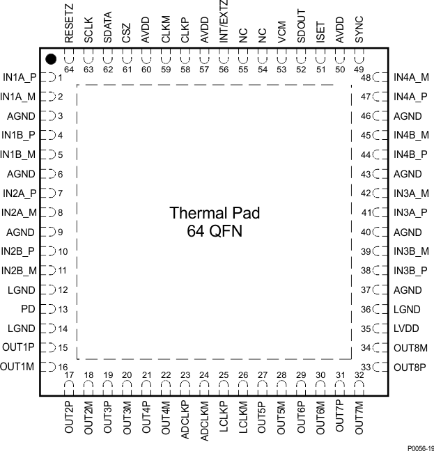
| ADCLKM |
24 |
O |
LVDS frame clock (1X) – negative output |
| ADCLKP |
23 |
O |
LVDS frame clock (1X) – positive output |
| AGND |
3, 6, 9, 37,
40, 43, 46 |
I |
Analog ground |
| AVDD |
50, 57, 60 |
I |
Analog power supply, 3.3 V |
| CLKM |
59 |
I |
Negative differential clock input. For single-ended clock, tie CLKM to ground. |
| CLKP |
58 |
I |
Positive differential clock input |
| CS |
61 |
I |
Serial interface enable input, active LOW. The pin has an internal 300-kΩ pulldown resistor to ground |
| IN1A_P, IN1A_M |
1, 2 |
I |
Differential analog input for channel 1, 16 bit ADC |
| IN1B_P, IN1B_M |
4, 5 |
I |
Differential analog input for channel 1, 14 bit ADC |
| IN2A_P, IN2A_M |
7, 8 |
I |
Differential analog input for channel 2, 16 bit ADC |
| IN2B_P, IN2B_M |
10, 11 |
I |
Differential analog input for channel 2, 14 bit ADC |
| IN3A_P, IN3A_M |
41, 42 |
I |
Differential analog input for channel 3, 16 bit ADC |
| IN3B_P, IN3B_M |
38, 39 |
I |
Differential analog input for channel 3, 14 bit ADC |
| IN4A_P, IN4A_M |
47, 48 |
I |
Differential analog input for channel 4, 16 bit ADC |
| IN4B_P, IN4B_M |
44, 45 |
I |
Differential analog input for channel 4, 14 bit ADC |
| INT/EXT |
56 |
I |
Internal/external reference mode select input
Logic HIGH –internal reference
Logic LOW – external reference |
| ISET |
51 |
I |
Bias pin – 56.2 kΩ resistor (1% tolerance value) to ground |
| LCLKM |
26 |
O |
LVDS bit clock (8X) – negative output |
| LCLKP |
25 |
O |
LVDS bit clock (8X) – positive output |
| LGND |
12, 14, 36 |
I |
Digital ground |
| LVDD |
35 |
I |
Digital and I/O power supply, 1.8 V |
| OUT1P, OUT1M |
15, 16 |
O |
Wire 1, channel 1 LVDS differential output |
| OUT2P, OUT2M |
17, 18 |
O |
Wire 2, channel 1 LVDS differential output |
| OUT3P, OUT3M |
19, 20 |
O |
Wire 1, channel 2, LVDS differential output |
| OUT4P, OUT4M |
21, 22 |
O |
Wire 2, channel 2 LVDS differential output |
| OUT5P, OUT5M |
27, 28 |
O |
Wire 1, channel 3 LVDS differential output |
| OUT6P, OUT6M |
29, 30 |
O |
Wire 2, channel 3 LVDS differential output |
| OUT7P, OUT7M |
31, 32 |
O |
Wire 1, channel 4 LVDS differential output |
| OUT8P, OUT8M |
33, 34 |
O |
Wire 2, channel 4 LVDS differential output |
| PD |
13 |
I |
Power-down input |
| NC |
54, 55 |
|
Do not connect |
| RESET |
64 |
I |
Serial interface RESET input, active LOW.
When using the serial interface mode, the user must initialize internal registers through hardware RESET by applying a low-going pulse on this pin or by using software reset option. See the Serial Interface section. |
| SCLK |
63 |
I |
Serial interface clock input. The pin has an internal 300-kΩ pulldown resistor. |
| SDATA |
62 |
I |
Serial interface data input. The pin has an internal 300-kΩ pulldown resistor. |
| SDOUT |
52 |
O |
Serial register readout
This pin is in the high-impedance state after reset. When the <READOUT> bit is set, the SDOUT pin becomes active. This is a CMOS digital output running from the AVDD supply. |
| SYNC |
49 |
I |
Input signal to synchronize channels and chips when used with reduced output data rates
Alternate function: Clamp signal input (14-bit ADC mode only) |
| VCM |
53 |
IO |
Internal reference mode: Outputs the common-mode voltage (1.5 V) that can be used externally to bias the analog input.
External reference mode: Apply voltage input that sets the reference for ADC operation. |
