SBAS948B December 2018 – September 2025 ADS52J65 , ADS52J66
PRODUCTION DATA
- 1
- 1Features
- 2Applications
- 3Description
- 4Device and Documentation Support
- 5Revision History
- 6Mechanical, Packaging, and Orderable Information
Package Options
Mechanical Data (Package|Pins)
- RGC|64
Thermal pad, mechanical data (Package|Pins)
- RGC|64
Orderable Information
3 Description
The 8/4-channel, 16/14-bit ADS52J6x analog-to-digital converter (ADC) uses CMOS process and remarkable circuit techniques. The device is designed to operate at low power and give very high signal-to-noise ratio (SNR) performance with a 2-Vpp full-scale input. The ADS52J65 device gives 80dBFS idle SNR and 78dBFS full scale SNR at 5MHz. The large input bandwidth of 250MHz makes the device well suited for a wide range of applications, such as high frequency medical ultrasound, magnetic resonance imaging, multi-channel data acquisition, flow cytometry, and hematology analyzer. The ADC integrates an internal reference trimmed to match across devices.
| Part Number | Resolution | Number of Channels |
|---|---|---|
| ADS52J65 | 16-bit | 8 |
| ADS52J66 | 14-bit | 8 |
| ADS52J67 | 16-bit | 4 |
| ADS52J68 | 14-bit | 4 |
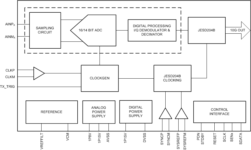
ADS52J6x has advanced digital features, including a digital I/Q demodulator with fractional decimation filter. The ADC data from each channel is encoded using an 8B to 10B format and is sent as a SerDes data stream using current-mode logic (CML) outputbuffers, as per the JESD204B standard. The ADC data from all eight channels can be output over a single CML buffer (1-lane SerDes) with the data rate limited to a maximum of 12.8Gbps. Using SerDes outputs reduces the number of interface lines. This, together with the low-power design, enables eight channels to be packaged in a 9mm × 9mm VQFN allowing high system integration densities. ADS52J6x also supports modes where all ADC data is sent over four CML buffers (4-Lane SerDes), reducing the SerDes data rate per lane for low-cost FPGAs. The ADS52J6x is available in a non-magnetic VQFN package that does not create any magnetic artifact. The device is specified over –40°C to +85°C.
 Block
Diagram