SLAS918B December 2012 – April 2022 ADS54T01
PRODUCTION DATA
- 1 Features
- 2 Applications
- 3 Description
- 4 Revision History
- 5 Device Comparison
- 6 Pin Configuration and Functions
- 7 Specifications
-
8 Detailed Description
- 8.1 Overview
- 8.2 Functional Block Diagram
- 8.3
Feature Description
- 8.3.1 Test Pattern Output
- 8.3.2 Clock Inputs
- 8.3.3 SNR and Clock Jitter
- 8.3.4 Analog Inputs
- 8.3.5 Over-Range Indication
- 8.3.6 Interleaving Correction
- 8.3.7 High-Resolution Output Data
- 8.3.8 Low-Resolution Output Data
- 8.3.9 Full Speed – 7 Bit
- 8.3.10 Decimated Low-Resolution Output Data
- 8.3.11 Multi Device Synchronization
- 8.4 Device Functional Modes
- 8.5 Programming
- 8.6 Register Maps
- 9 Power Supply Recommendations
- 10Device and Documentation Support
- 11Mechanical, Packaging, and Orderable Information
Package Options
Mechanical Data (Package|Pins)
- ZAY|196
Thermal pad, mechanical data (Package|Pins)
Orderable Information
8.4.5 Auto Trigger Mode
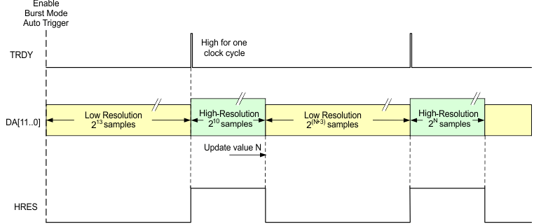
This mode is enabled by setting the auto trigger bit through a SPI register write and the DA data outputs start in low resolution for 213 samples. Immediately following completion of transmission of the last low resolution sample, the outputs automatically start transmitting 210 high-resolution samples without the need for external trigger ensuring maximum efficiency. Any input signal on the TRIGGER pins is ignored and the TRDY flag will go high only for one clock cycle with the start of the high-resolution data.
The output flag HRES is aligned with the 2N high-resolution output samples and the parameter N can be changed until the next output cycle starts again with low-resolution output data.
 Figure 8-18 Auto Trigger Mode Timing Diagram